OEM & ODM PCB/PCBA Manufacturing — From Design Support to Reliable Mass Production
- HDI / Rigid-Flex / Controlled Impedance / Via-in-Pad
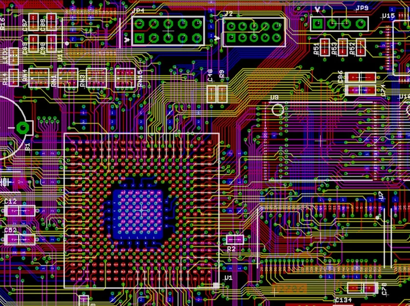
- DFM & stackup co-design; fast, practical engineering feedback
- Full traceability, IPC/ISO-based QA, panel-level impedance coupons
- Turn-key sourcing or consigned kits with clear substitution rules
- Transparent lead times and yield-driven quoting
OEM vs. ODM — Which Model Fits Your Project?
| Topic | OEM (Build-to-Print) | ODM (Co-Design & Customization) |
|---|---|---|
| Design ownership | You provide complete design (Gerber/ODB++/IPC-2581, BOM, PnP, STEP) | We help define stackup, parts, substitutions; schematic/layout if needed |
| Change control | Based on your documents; engineering review before release | Joint milestones (PRD → EVT → DVT → PVT) and formal ECO flow |
| Cost & schedule | Faster onboarding, predictable cost | More engineering upfront, better manufacturability & lifetime cost |
| Best for | Mature designs, repeat orders, clear test specs | New products, rapid validation, BOM cost/Yield optimization |
Engagement Models
1) OEM — Build-to-Print
Input: full design package.
Output: traceable production, 100% E-test, X-ray where needed, stable mass delivery.
2) ODM — Co-Design & Manufacturing
Input: functional targets, interfaces, environment/reliability, budget & timeline.
Output: stackup/material proposal, key component selection/substitution list, layout constraints, prototypes & validation, ramp-to-mass plan.
Process & Quality Control
- DFM/DFT early lock-in: min line/space, vias (uVia/VIP/back-drill), annular ring, impedance tolerance.
- Materials & stackups: selected by signal/power/thermal needs; low-loss or hybrid options when required.
- Manufacturing: LDI imaging, laser microvias, resin/copper fill & cap, sequential lamination, controlled impedance.
- Inspection & test: AOI (inner/outer), flying-probe/ICT, BGA X-ray, TDR coupons per panel, FCT as specified.
- Traceability: lot-to-material-to-test data linkage; first-article & in-process checkpoints.
IP & Confidentiality
- Mutual NDA; least-privilege file access.
- Project-level data segregation and retention per your policy.
- Optional file encryption/version control and audit logs.
Deliverables
- Fabrication: final stackup, impedance/TDR report, key dimension report, first-article/process checks.
- Assembly: reflow profile, X-ray report, approved alternates list (if any).
- Test: FCT/ICT logs, unique SNs with timestamps, programming records.
- Certificates: RoHS/REACH declarations, COC/COA; material compliance on request.
Lead-Time Bands (typical)
- PCB prototypes: X–Y working days (by layer/complexity).
- Turn-key PCBA prototypes: X–Y working days after materials are complete.
- Pilot/MP: SLA and capacity curve after BOM lock & tooling.
Expedite options available after yield/feasibility review.
Sourcing & Substitution Rules
- Turn-key: we procure full BOM with incoming inspection.
- Consigned/partial: you supply critical ICs or custom parts; we complete the rest.
- Substitutions: only same footprint and equal/higher spec; written approval required. No substitutions for key ICs unless explicitly allowed.
Test & Programming
- Test matrix per project: flying-probe / ICT / boundary scan / FCT.
- Target coverage and pass/fail thresholds defined up front.
- Firmware programming and serialization: unique SN, QR/1D labels, log format agreed.
OEM/ODM RFQ Checklist
OEM: Gerber/ODB++/IPC-2581, BOM with MPNs & substitution policy, PnP/XY, STEP, assembly drawings, test spec, target lead time & quantities.
ODM: PRD (functions, interfaces, power), performance/reliability targets, environment & certifications (e.g., automotive/medical), cost & delivery goals, prototype schedule (EVT/DVT/PVT).
FAQs
Q1. Can you mix materials for low-loss/high-speed layers?
Yes. We can use low-Dk/Df for high-speed layers and high-TG FR-4 elsewhere, with thermal/warpage analysis and defined process windows.
Q2. How do you control impedance tolerance?
Stackup and copper thickness locked before release; TDR coupons per panel; typical ±10%, tighter on validated builds.
Q3. Does via-in-pad impact lead time?
VIP (fill & cap) adds processes/cure time. Use VIP only where density demands it and standard vias elsewhere to balance cost/lead time.
Q4. Do you support small-batch, high-mix NPI?
Yes. We recommend staged ramp with shared fixtures/stencils to balance speed and yield.
Q5. How are alternates approved?
By written rules agreed at RFQ. All alternates require engineering + purchasing sign-off with returned BOM change records.
Get OEM/ODM Quote — Upload Gerber/ODB++ (or your PRD for ODM). We’ll return a manufacturable plan with lead time and yield-aware pricing.