Procedures and Practical Strategies for Improving Testability in PCB Circuit Design
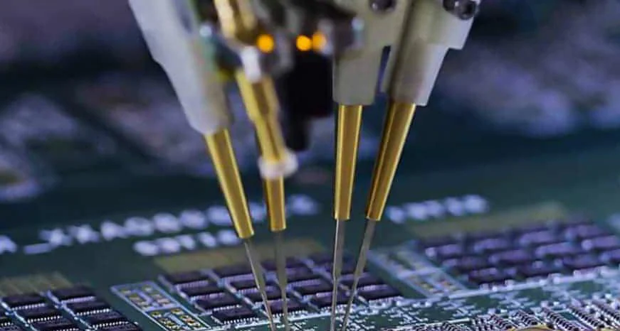
With continuous advancements in electronic technology, particularly the emergence of miniaturized and highly integrated components, the insulation spacing between conductors in micro-ICs like BGA packages has shrunk to 0.5mm. These technological innovations have made circuit design and testing for electronic products increasingly complex. This article introduces several design procedures and practical strategies to enhance PCB testability, helping you reduce production testing costs and improve product quality.
1. What is Design for Testability (DFT)?
Testability refers to the ability to verify component functionality and performance through straightforward testing methods, ensuring they operate as intended. In PCB circuit design, improving testability means:
Simplifying the testing process: Ensuring test methods are straightforward so engineers can quickly verify circuit components.
Accelerating test program development: Enabling rapid test program creation to save time and costs.
Comprehensive fault diagnosis: Promptly identifying and diagnosing circuit defects.
Convenient test point access: Designing easily accessible test points for subsequent testing.
To achieve optimal testability, both mechanical and electrical design requirements must be considered during the design phase. While implementing testability may incur some costs, it significantly boosts production efficiency, reduces testing and repair expenses, and is crucial for successful manufacturing.
2. Why Adopt Test-Friendly PCB Circuit Design?
Historically, if a product failed testing, issues were often deferred to later stages. Modern design philosophy emphasizes early detection and resolution—particularly of defects identifiable during production testing—to prevent their overlooking in functional or system testing.
Modern products are highly complex, and certain manufacturing defects may remain undetected even during functional testing. For instance, components requiring pre-programming—such as flash memory or in-system programmable devices (ISP)—must have their programming requirements addressed during the design phase. Test-friendly design helps identify and resolve these issues early, preventing additional production and repair expenses.
Although a test-friendly design may incur some initial costs, it facilitates early fault detection, ultimately saving substantial expenses later. In practice, testing costs increase exponentially with each additional test level, potentially rising tenfold per tier. Thus, test-friendly design significantly reduces overall testing expenses.
3. How do documentation materials impact circuit testability?
Circuit design testability heavily relies on comprehensive development documentation and component functional specifications. Test engineers require detailed knowledge of component specifications and functions to develop effective test procedures. Close collaboration between the design and test phases is crucial to ensure the completeness of test documentation.
The documentation required for testing includes:
Bill of Materials (BOM): Lists all components and assemblies.
Circuit design schematics (e.g., CAD data): Provide detailed information on component layout and connections.
Component functional documentation (e.g., datasheets): Assist test engineers in understanding each component's functionality and operation.
For programmable components (e.g., FPGAs, PLDs, flash memory), pre-programming within the test system is a critical step to enhance testability. Ensuring programming data integrity prevents test failures caused by data conflicts.
4. How Does Test-Friendly PCB Design Reduce Costs?
Although investing more resources in test-friendly design during the circuit design phase may increase initial costs, it reduces testing complexity during production and lowers overall testing and repair expenses. Test-friendly design enables more efficient production lines and helps companies minimize repair costs arising from delayed defect detection.
By adhering to testability design guidelines, engineers can identify potential issues early and address them promptly through precise testing procedures. This approach not only improves product quality in the long run but also significantly boosts production efficiency.
Benchuang Electronics offers high-quality PCB Design and High-Speed PCB services. Contact us and send your specifications.

