Pads, the fundamental building blocks of surface mount assembly, form the land pattern on a PCB. This pattern consists of various pad combinations designed for specific component types. Pads serve as partially conductive patterns for electrical connections, device fixation, or both.
Pad geometry may vary depending on the type of soldering used for mounting electronic components. Where possible, pad shapes should be defined in a manner transparent to the mounting process employed. Whether components are mounted on one or both sides of the board, subjected to wave, reflow, or other soldering processes, pads and component dimensions should be optimized to ensure proper solder joint formation and compliance with inspection standards. Although pad patterns are defined dimensionally and form part of the printed circuit board geometry, they are constrained by manufacturability levels and tolerances related to plating, etching, assembly, or other conditions. The use of solder mask and alignment between the solder mask and conductor patterns also influences manufacturability.

1. Pad Requirements
The International Electrotechnical Commission (IEC) Standard 61188 recognizes the need for different objectives regarding solder fillet or pad protrusion conditions. This new international standard confirms two fundamental approaches for developing pad shapes:
1) Accurate data based on industrial component specifications, PCB manufacturing capabilities, and component placement precision. These pad shapes are specific to a particular component and are identified by a pad shape number.
2) Equations that can be used to modify given information to achieve a more robust solder joint. This is applicable in special cases where the precision of placement or mounting equipment varies more or less than assumed when determining pad details.
The standard defines maximum, medium, and minimum material conditions for pads used to mount various pins or component terminals. Unless otherwise specified, this standard designates all three “desired targets” as Level 1, Level 2, or Level 3.
Level 1: Maximum – For low-density product applications, the “maximum” pad condition is used for wave or reflow soldering of leadless chip components and finned components with leads. The geometry configured for these components, as well as inward-facing “J”-type lead components, provides a wider process window for manual soldering and reflow soldering.
Level 2: Medium – Products with moderate component density may consider this “medium” pad geometry. Closely resembling the IPC-S-782 standard pad geometry, medium pads configured for all component types provide robust soldering conditions for reflow processes and should offer adequate conditions for wave or flow soldering of leadless and wing-lead components.
Level 3: Minimal – Products with high component density (typically portable applications) may consider the “minimal” pad geometry. Minimal pad geometry selection may not be suitable for all products. Before adopting minimal pad shapes, product constraints should be considered and testing conducted based on the conditions outlined in the table.
Pad geometries provided in IPC-SM-782 and defined in IEC 61188 should accommodate component tolerances and process variations. While the pads in the IPC standard provide a robust interface for most assembly applications, some companies have expressed the need for minimal pad geometries for portable electronics and other unique high-density applications.
The international pad standard (IEC 61188) recognizes the requirements of higher component density applications and provides information on pad geometries for specific product types. This information aims to specify appropriate dimensions, shapes, and tolerances for surface-mount pads to ensure sufficient area for proper solder fillet formation while also allowing inspection, testing, and rework of these solder joints.

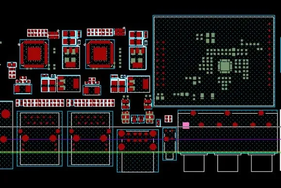
2. BGA and CAP
BGA packaging has evolved to meet current solder mounting techniques. Plastic and ceramic BGA components feature relatively wide contact pitches (1.50, 1.27, and 1.00 mm), while chip-scale BGAs have grid pitches of 0.50, 0.60, and 0.80 mm. Both standard BGAs and fine-pitch BGAs are less prone to damage compared to ICs in fine-pitch pinframe packages. The BGA standard permits selective reduction of contact points to meet specific input/output (I/O) requirements. When establishing contact point layouts and lead arrangements for BGA components, package developers must consider chip design alongside the dimensions and shape of the chip block. Another issue encountered during technical lead arrangement is chip orientation (whether the chip module's pads face upward or downward). The “face-up” configuration for chip modules is typically employed when suppliers utilize COB (chip-on-board) technology.
Component construction and the materials used in its manufacture are not defined within this industry standard and guideline. Each manufacturer will strive to tailor its specific structure to meet the application requirements defined by the user. For example, consumer products may operate in relatively benign environments, while industrial or automotive applications often demand performance under more severe stress conditions. Depending on the physical properties of the materials selected for manufacturing the BGA, flip-chip or wire-bonding techniques may be employed. Since the chip mounting structure is rigid, the chip module mounting base is typically centered with conductors, with signals routed from the chip module pads into an array of contact balls.

The grid array package outlined in this document is provided in JEDEC Publication 95. Square BGAs: JEDEC MS-028 defines a smaller rectangular plastic BGA component category with a contact pitch of 1.27 mm. The overall outline dimensions of this matrix component allow significant flexibility, such as pin spacing, contact matrix layout, and construction. JEDEC MO-151 defines various plastic-encapsulated BGAs. Square profiles cover dimensions from 7.0 to 50.0, with three contact pitch options: 1.50, 1.27, and 1.00 mm.
Ball contacts may be distributed in a single pattern, with rows and columns arranged in even or odd numbers. While the arrangement must maintain symmetry across the entire package outline, component manufacturers are permitted to reduce contact locations within specific areas.
Benchuang Electronics offers high-quality PCB layout and High-Speed PCB services. Contact us and send your specifications.