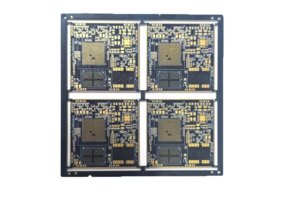
Multilayer PCBs are printed circuits made up of more than two layers. They must therefore have at least three layers of conductive material within the insulating material.And they allow the creation of circuits with reduced dimensions, with a considerable saving of space and weight, the external wiring is reduced to a minimum, the electronic components can be mounted by adhering to a higher assembly density
Multilayer PCBs are printed circuit boards built by laminating three or more copper layers with insulating dielectrics in between. Inner signal layers and dedicated power/ground planes let you route complex circuits in a compact footprint while improving electrical stability and EMI performance.
If your design is limited by routing density, noise, high-speed signals, or power distribution, moving from 2-layer to multilayer is often the most effective step.
1) Multilayer vs. Double-Sided (Why Buyers Upgrade)
Item
Multilayer PCB
Double-Sided PCB
Routing capacity
Much higher via inner layers
Limited to top/bottom
SI/PI stability
Easier with dedicated planes
Harder to isolate noise
EMI control
Better shielding with planes
More exposed signal paths
Product size
Smaller boards for same function
Larger boards needed
Typical need
Complex / dense / high-speed designs
Moderate complexity
2) What Multilayer PCBs Enable in Real Designs
Multilayer stackups are chosen when you need one or more of these outcomes:
High-density routing for compact devices and fine-pitch components
Controlled impedance for high-speed or RF signal paths
Cleaner power distribution using power/ground planes
Lower EMI and crosstalk through layer separation and shielding
Mechanical stability for assemblies that must survive thermal or vibration stress
3) Stack-Up Basics (How Layers Work Together)
A multilayer board usually includes a mix of:
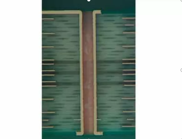
Outer layers: component pads + main signal routing
Optional via structures: through-vias, blind/buried vias, or microvias to increase density and shorten signal paths
The right stackup is driven by routing density, impedance targets, EMI risk, and your assembly constraints.
4) When You Should Choose Multilayer
Multilayer PCBs are a strong fit when:
Two layers can’t finish routing without risky trace compromises
You need high-speed interfaces (and stable impedance)
EMI or grounding issues show up in early prototypes
The enclosure is tight and board size must shrink
Power delivery is sensitive and needs dedicated planes
Reliability requires stable thermal and mechanical behavior
5) DFM Tips to Improve Yield & Electrical Performance
Plan the stackup before final routing Lock dielectric thickness, copper distribution, and plane order early. Late stackup changes are a top cause of redesign loops.
Use planes to control return paths High-speed signals should reference continuous ground planes to reduce noise and radiation.
Keep critical nets in stable process windows Avoid pushing every trace to the minimum possible width/space unless necessary—yield drops fast at the edge.
Manage via strategy for SI and cost Use advanced vias (blind/buried or microvias) only where they deliver real density or SI benefit; otherwise, standard vias keep cost down.
Balance copper to reduce warpage Symmetric copper distribution helps prevent twist/bow, improving assembly yield.
6) Key Cost Drivers (What Changes Price Fast)
Layer count and stackup complexity
Special via structures (blind/buried/microvia vs. standard through-vias)
Material grade needs (high-TG, low-loss, halogen-free, etc.)
Impedance control requirements
Copper weight and any heavy-copper zones
Board outline complexity and panel utilization
Surface finish choice and test coverage
A short DFM review usually identifies which drivers can be optimized without sacrificing performance.
Prototype build → verify assembly and electrical stability
Pilot run → validate yield and repeatability
Mass production → stable delivery with full process control
Early DFM alignment reduces both cost and schedule risk.
8) RFQ Checklist (Send This for a Fast, Accurate Quote)
RFQ Item
What to provide
Why it matters
Design files
Gerber or ODB++
Confirms routing density & features
Target stackup
Layer order, dielectric plan, copper weights
Validates manufacturability & SI/PI
Impedance needs
Controlled-impedance nets & targets
Locks process route
Via needs
Through-via only or blind/buried/microvia zones
Drives cost & yield
Reliability targets
Test or standard requirements
Sets material & validation level
Quantity plan
Prototype / MPQ / annual volume
Optimizes panel strategy & lead time
Assembly notes
Finish, component side, special constraints
Prevents build surprises
Ready to Start Your Multilayer PCB Project?
Multilayer PCBs are the fastest way to increase routing density, clean up signal/power integrity, and shrink board size in complex electronics. Send your Gerber + target stackup + impedance requirements for a quick DFM review and quotation. Early agreement on stackup and via strategy is the shortest path to stable prototypes and smooth mass production.