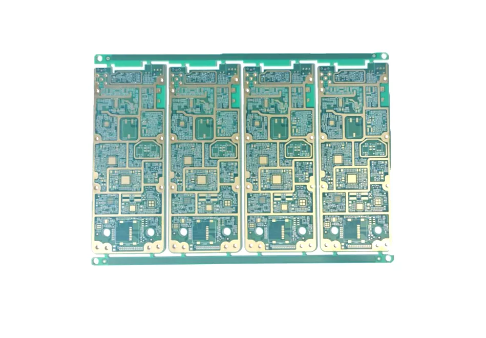
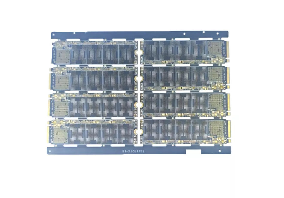
High-density interconnect, or HDI, circuit boards are printed circuit boards with a higher wiring density per unit area than traditional printed circuit boards. In general, HDI PCBs are defined as PCBs with one or all of the following: microvias; blind and buried vias; built-up laminations and high signal performance considerations. Printed circuit board technology has been evolving with changing technology that calls for smaller and faster products. HDI boards are more compact and have smaller vias, pads, copper traces and spaces. As a result, HDIs have denser wiring resulting in lighter weight, more compact, lower layer count PCBs. Rather than using a few PCBs in a device, one HDI board can house the functionality of the previous boards used.
The primary benefit of HDI printed circuit boards is the capability to “do more with less”; with copper-etching technology continuously refined for better precision, it became possible to combine functionalities of multiple PCBs into one HDI PCB.
Feature
Technical specification
Number of layers
4 – 22 layers standard, 30 layers advanced
Technology highlights
Multilayer boards with a higher connection pad density than standard boards, with finer lines/spaces, smaller via holes and capture pads allowing microvias to only penetrate select layers and also be placed in surface pads.
HDI builds
1+N+1, 2+N+2, 3+N+3,4+N+4, any layer / ELIC, Ultra HDI in R&D
Materials
FR4 standard, FR4 high performance, Halogen free FR4, Rogers
Copper weights (finished)
18μm – 70μm
Minimum track and gap
0.075mm / 0.075mm
PCB thickness
0.40mm – 3.20mm
Maxmimum dimensions
610mm x 450mm; dependant upon laser drilling machine
High Density Interconnect (HDI) PCBs are advanced printed circuit boards engineered for higher wiring density per unit area than conventional multilayer boards. By using laser-drilled microvias, fine-line imaging, and blind/buried via structures, HDI enables compact layouts, shorter signal paths, and better performance in high-speed and high-IO designs.
At Benchuang Electronics in Shenzhen, HDI is one of our core production categories. We support projects from early prototype validation to stable mass production with a manufacturing system focused on microvia integrity, fine-line yield, and lamination registration.
Why Choose HDI PCBs?
Smaller size with more functions in the same footprint
Better high-speed signal integrity with shorter interconnect length and lower parasitic effects
Reliable routing for high-pin-count packages such as fine-pitch BGA and SiP modules
Increased reliability versus using multiple connectors and cables in compact products
HDI technology allows you to achieve aggressive form-factor and performance targets without splitting the design into multiple boards and harnesses.
Benchuang HDI Manufacturing Capabilities
1. Microvia Drilling & Filling Reliability
Laser-drilled microvias down to approximately 0.10 mm
Closed-loop control of laser energy for stable via geometry
High microvia filling rate, helping ensure long-term signal and mechanical reliability
2. Fine-Line Imaging
Fine-line routing in the 3/3 mil (≈0.075/0.075 mm) class
Laser Direct Imaging (LDI) used for critical HDI layers
Controlled etch uniformity to support high-yield mass production on dense designs
3. Lamination Registration
Multi-cycle lamination with optical alignment
Layer-to-layer registration controlled to tight tolerances, suitable for fine-pitch BGA pads and via-in-pad structures
4. Materials & Stack-Up Support
Stable sourcing of HDI-grade laminates and prepregs
Stack-up design support including Tg, CTE, Dk and Df evaluation
Engineering guidance for high-speed, RF-HDI or mixed-material stack-ups
5. Capacity & Lead Time
HDI production capacity suitable for both prototype and volume orders
Typical HDI lead times optimized for global customers
Process control and yield management aimed at consistent quality and on-time delivery
HDI Structures We Produce
Benchuang manufactures mainstream HDI build types used in today’s compact high-IO electronics, including:
1+N+1, 2+N+2 and other build-up structures
Staggered microvias and stacked microvias
Blind and buried via combinations
Via-in-pad with resin plug and copper cap for fine-pitch BGA and RF front-ends
If your design uses special materials (low-loss, high-Tg, halogen-free, RF hybrid), our engineers can recommend stack-ups that balance electrical performance, reliability and cost.
Quality Control for HDI Boards
HDI reliability depends on a few critical points. Our quality system is built around them:
Incoming Inspection & Traceability
Each panel is assigned a unique ID linked to material and process records
Full traceability from laminate lot to final shipment
In-Process SPC at Critical Steps
Statistical process control on laser drilling, plating and lamination
Tight control of copper plating thickness and microvia filling
Routine measurement of critical dimensions and registration
Final Electrical & Reliability Verification
100% electrical testing (flying-probe or fixture)
Cross-sections and X-ray inspection on representative lots
Reliability tests available for automotive and medical projects on request
Typical HDI Applications
HDI PCBs are widely used where space, speed and reliability must all be optimized:
AI and high-performance computing modules
5G and telecom infrastructure, RF front-end boards
Medical imaging equipment and portable medical devices
Automotive ADAS, ECU and sensor-fusion modules
Consumer electronics, wearables and compact handheld devices
These applications benefit from shorter signal paths, higher layer density, and robust microvia structures.
DFM & Quotation Support
To help engineers and buyers move quickly from concept to production, Benchuang provides:
Free DFM review for HDI stack-ups, microvia design, via-in-pad options and key cost drivers
Engineering feedback within a short response window for most RFQs
Prototype-to-volume roadmaps, so you can keep the same factory from EVT/DVT to mass production
Our goal is to make HDI manufacturability clear early in the design phase, reduce redesign cycles, and give you predictable cost and lead-time windows.
Get a Fast HDI Feasibility Review
Send us your Gerber files, stack-up requirements and target application. Our engineering team will provide:
A quick manufacturability check
Suggested HDI build type (1+N+1, 2+N+2, stacked or staggered microvias, via-in-pad, etc.)
Material and surface-finish recommendations
A quotation window from prototype to potential volume production