Multilayer PCBs are printed circuits made up of more than two layers. They must therefore have at least three layers of conductive material within the insulating material.And they allow the creation of circuits with reduced dimensions, with a considerable saving of space and weight, the external wiring is reduced to a minimum, the electronic components can be mounted by adhering to a higher assembly density
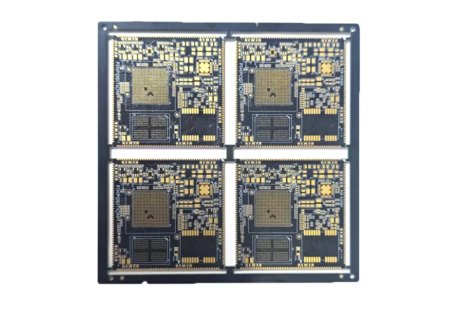
Multilayer PCBs are printed circuit boards built by laminating three or more copper layers with insulating dielectrics in between. Inner signal layers and dedicated power/ground planes let you route complex circuits in a compact footprint while improving electrical stability and EMI performance.
If your design is limited by routing density, noise, high-speed signals, or power distribution, moving from 2-layer to multilayer is often the most effective step.