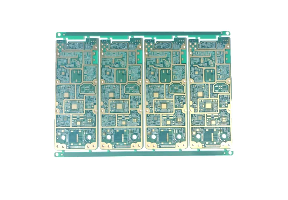
High-density interconnect, or HDI, circuit boards are printed circuit boards with a higher wiring density per unit area than traditional printed circuit boards. In general, HDI PCBs are defined as PCBs with one or all of the following: microvias; blind and buried vias; built-up laminations and high signal performance considerations. Printed circuit board technology has been evolving with changing technology that calls for smaller and faster products. HDI boards are more compact and have smaller vias, pads, copper traces and spaces. As a result, HDIs have denser wiring resulting in lighter weight, more compact, lower layer count PCBs. Rather than using a few PCBs in a device, one HDI board can house the functionality of the previous boards used.
The primary benefit of HDI printed circuit boards is the capability to “do more with less”; with copper-etching technology continuously refined for better precision, it became possible to combine functionalities of multiple PCBs into one HDI PCB.