During PCB Layout, how can we ensure efficient operation of flash memory and other programmable components?
Flash memory programming can sometimes take a long time (up to 1 minute for large memories or memory banks). Therefore, reverse drive from other components must be prevented during this period, as it could damage the flash memory. To avoid this, all components connected to the address bus control lines must be placed in a high-impedance state. Similarly, the data bus must also be capable of being isolated to ensure the flash memory is unloaded and ready for subsequent programming.
In-system programmable (ISP) components, such as those from Altera, Xilinx, and Lattice, have specific requirements, as well as other special considerations. Beyond ensuring mechanical and electrical testability prerequisites, the capability for programming and verification data must be guaranteed. For Altera and Xilinx components, the Serial Vector Format (SVF) is employed, which has recently evolved into a near-industry standard. Many test systems can program such devices and utilize input data within the SVF for generating test signals.
Programming these devices via the Boundary-Scan Chain (JTAG) also employs the serial data format. When compiling programming data, it is crucial to consider the entire device chain within the circuit; data should not be reduced solely to the device being programmed. During programming, the automated test signal generator accounts for the entire component chain and incorporates other components into a bypass model.
Conversely, Lattice requires data in JEDEC format and performs parallel programming through standard input and output ports. Post-programming, the data is also used to verify component functionality. Data provided by the development department should be as readily usable as possible by the test system directly, or with minimal conversion.
What to Consider for Boundary Scan (JTAG)
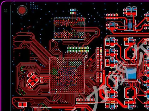
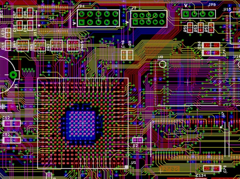
Components composed of intricate grids based on complex elements provide test engineers with only a limited number of accessible test points. Even in such cases, testability can still be enhanced. Boundary scan and integrated self-test (IST) technologies can be employed to reduce test completion time and improve test effectiveness.
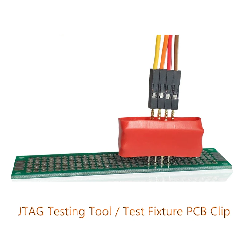
For both development and test engineers, establishing a test strategy based on boundary scan and IST technologies inevitably increases costs. Development engineers must incorporate boundary scan components (IEEE-1149.1 standard) into the circuit and ensure specific test pins are accessible (e.g., Test Data Input - TDI, Test Data Output - TDO, Test Clock - TCK, Test Mode Select - TMS, and possibly Test Reset).
Test engineers create a boundary scan description language (BSDL) model for the device. At this stage, they must know which boundary scan functions and commands the device supports. Boundary scan testing can diagnose shorts and opens down to the wire level. Additionally, if specified by the development engineer, the component's built-in self-test (BIST) can be triggered via the boundary scan command “RunBIST.” Particularly in circuits containing numerous ASICs and other complex components where conventional test models are unavailable, boundary scan components can significantly reduce the cost of developing test models.
The extent of time and cost reduction varies per component. For a circuit containing an IC requiring 100% fault coverage, approximately 400,000 test vectors are typically needed. By employing boundary scan, the number of test vectors can be reduced to a few hundred while maintaining the same fault coverage rate. Therefore, the boundary scan approach offers distinct advantages when test models are unavailable or access to circuit nodes is restricted. The decision to adopt boundary scan depends on balancing the increased costs during development, utilization, and manufacturing. Boundary scan must be weighed against the required fault detection time, test time, time-to-market, and adapter costs, aiming for maximum cost savings. In many cases, a hybrid approach combining traditional in-circuit test methods with boundary scan proves to be the optimal solution.
Benchuang Electronics offers high-quality PCB layout and High-Speed PCB services. Contact us and send your specifications.