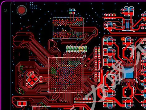
I. Determining Loop Area Based on Radiation
The reflection characteristics of open-ended transmission lines dictate the maximum line length. Due to mandatory requirements for product EM radiation, both the loop area and line length are constrained. When using an unshielded enclosure, these constraints are directly implemented by the PCB.
- Note: When employing series termination loads in asynchronous logic circuit design, quasi-stability must be considered. Symmetrical logic input circuits cannot determine whether the input signal is high or low, potentially leading to undefined output conditions.
For logic signals in the frequency domain, the spectral current amplitude is inversely proportional to the square of the frequency beyond the logic signal bandwidth (= 1/π.τr). Expressed in angular frequency, the loop's radiated impedance remains proportional to the square of the frequency. Consequently, the maximum loop area can be calculated, determined by the clock rate or repetition rate, the logic signal's rise time or bandwidth, and the time-domain current amplitude. The current waveform is determined by the voltage waveform, with the current half-width time approximately equal to the voltage rise time.
The current amplitude can be expressed in terms of angular frequency (=1/π·τ_r) as:
I(f) = 2·I·τ_r/T
Where:
I = Time-domain current amplitude;
T = Reciprocal of the clock rate, i.e., the period;
τ_r = Voltage rise time, approximately equal to the current half-width time τ_H.
This equation enables the calculation of the maximum loop area for a given logic family circuit at a specific clock rate. Table 5 provides corresponding loop areas. The maximum loop area is determined by the clock rate, logic circuit type (= output current), and the number n of concurrent switching loops on the PCB.
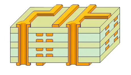
If the clock rate exceeds 30MHz, multilayer circuit boards must be used. In this case, the epoxy thickness varies with the number of layers, ranging from 60 to 300μm. Acceptable results on double-layer boards can be achieved only when the number of high-speed clock signals on the PCB is limited, through careful routing using layer-to-layer traces.
Note: In such cases, standard DIL packages may exceed loop area limits, necessitating additional shielding measures and appropriate filtering.
All connectors linking to other panels and components must be placed as close together as possible. This prevents common-mode currents conducted through cables from flowing into PCB circuit traces and avoids voltage drops between reference points on the PCB from exciting (antenna) cables.
To avoid this common-mode interference, the reference ground near the connector must be isolated from the ground plane, ground grid, or circuit reference ground on the PCB. Where possible, these ground planes should be connected to the product's metal enclosure. From this ground plane, only high-impedance components, such as inductors, resistors, reed relays, and optocouplers, may be connected between the two grounds. All connectors should be placed as close together as possible to prevent external currents from flowing through PCB traces or reference ground.
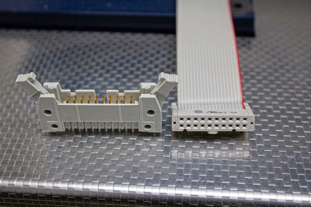
II. Proper Selection of Cables and Connectors in PCB Design
Cable selection is determined by the signal amplitude and frequency components flowing through the cable. For cables located outside the product, shielding is mandatory (per product requirements) when transmitting data signals with clock rates above 10kHz. The shielding section must be connected to ground at both ends of the cable (for products with metal enclosures) to ensure shielding against both electric and magnetic fields.
If separate grounding is used, connect to “connector ground” rather than “circuit ground.”
For clock rates between 10kHz and 1MHz, maintaining the lowest possible logic circuit rise time can achieve over 80% optical coverage or a transfer impedance below 10nH/m. Better shielded cables are required for clock rates exceeding 1MHz.
Generally, except for coaxial cables, the shielding of cables should not be used as a signal loop.
By inserting passive filters between signal inputs/outputs and ground/reference points to reduce RF components, high-quality shielding and corresponding connectors may not be necessary. Good shielded cables should be equipped with suitable connectors.
Benchuang Electronics offers high-quality PCB layout and High-Speed PCB services. Contact us and send your specifications.

