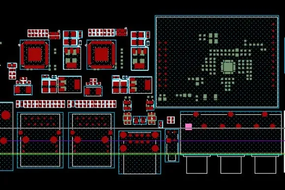
PCB routing significantly impacts the electromagnetic compatibility of the PCB. To ensure proper circuit operation on the PCB, routing should be optimized according to the constraints outlined in this document. This includes the layout of components/connectors and decoupling circuits used for certain ICs.
I. PCB Material Selection
By rationally selecting PCB materials and routing paths for printed circuits, transmission lines with low coupling to other lines can be achieved. When the distance d between transmission line conductors is smaller than the distance to adjacent conductors, lower coupling or reduced crosstalk can be attained.

Prior to design, the most economical PCB form can be selected based on the following criteria:
EMC requirements
· PCB density
· Assembly and manufacturing capabilities
· CAD system capabilities
· Design costs
· PCB quantity
· Electromagnetic shielding costs
When employing non-shielded enclosure product structures, particular attention should be paid to overall product cost/component packaging/pin configuration, PCB form factor, electromagnetic field shielding, construction, and assembly. In many cases, selecting an appropriate PCB form factor can eliminate the need for adding a metal shielding box within the plastic enclosure.
To enhance immunity for high-speed analog circuits and all digital applications while reducing harmful radiation, transmission line techniques are required. Depending on the output signal conversion, transmission lines between S-VCC, S-VEE, and VEE-VCC must be represented, as shown in Figure 1.
Signal current is determined by the symmetry of the circuit output stage. For MOS, IOL = IOH, while for TTL, IOL > IOH.
Function/Logic Type ZO(Ω)
Power Supply (Typical) <<10
ECL Logic 50
TTL Logic 100
HC(T) Logic 200
II. Signal Lines and Signal Loops
Signal lines should be routed as close as possible to their signal loops to prevent radiation from the enclosed loop area and reduce the magnetic permeability of the loop's induced voltage.
Typically, when the distance between two lines equals the line width, the coupling coefficient is approximately 0.5 to 0.6, reducing the effective self-inductance from 1 μH/m to 0.4–0.5 μH/m.
This implies that 40% to 50% of the signal loop current freely flows to other lines on the PCB.

During a transition from a high level to a low level in TTL logic circuits, the sink current exceeds the source current. In such cases, the transmission line is typically defined between Vcc and S, rather than between VEE and S. The use of ferrite rings allows complete control over the currents flowing in both the signal line and the signal return line.
For parallel conductors, the characteristic impedance of the transmission line is affected by the ferrite. In coaxial cables, however, the ferrite only influences the cable's external parameters.
Therefore, adjacent traces should be as narrow as possible, while vertically stacked traces should be the opposite (typically spaced less than 1.5mm/the thickness of epoxy in a double-layer board). Routing should place each signal trace and its return path as close as possible (applicable to both signal and power traces). If the coupling between transmission line conductors is insufficient, ferrite rings can be employed.
III. IC Decoupling
IC decoupling is typically achieved solely through capacitors. Since capacitors are imperfect, resonance may occur. Above the resonance frequency, capacitors behave like inductors, limiting the rate of change of current (di/dt). Capacitor values are determined by the allowable power supply voltage ripple between IC pins. Based on the practice of experienced designers, the voltage ripple should be less than 25% of the worst-case noise tolerance of the signal line.

For fast logic circuits, if the decoupling capacitor contains significant series inductance (which may result from the capacitor's structure, long leads, or PCB traces), the capacitance value may become ineffective. In such cases, an additional small ceramic capacitor (100-100 pF) should be added as close as possible to the IC pin, connected in parallel with the “LF-” decoupling capacitor. The resonant frequency of the ceramic capacitor (including the trace length to the IC power pin) should exceed the logic circuit's bandwidth [1/(π.τr)], where τr is the voltage rise time in the logic circuit.
When each IC has its own decoupling capacitor, signal loop currents can choose the most convenient path—VEE or VCC—determined by mutual coupling between signal traces and power traces.
A series resonant circuit forms between the two decoupling capacitors (one per IC) and the inductance Ltrace of the power trace. This resonance occurs only at low frequencies (<1MHz) or when the resonant circuit's Q-factor is low (<2).
By connecting a high-RF-loss choke coil in series between the Vcc network and the IC requiring decoupling, the resonant frequency can be maintained below 1 MHz. If the RF loss is too low, it can be compensated for by adding resistors in parallel or series.
The choke coil should always use an enclosed core; otherwise, it may become an RF transmitter or a magnetic field sensor.
Example: 1MHz*1μHz Z1=6.28Ω Rs=3.14Ω Q<2 Rp=12.56Ω
Above the resonant frequency, the characteristic impedance Z0 of the “transmission line” (where the IC's impedance is treated as a power supply load) equals: Z0 = √(Ltrace/Cdecoupling).
Benchuang Electronics offers high-quality PCB layout and High-Speed PCB services. Contact us and send your specifications.


