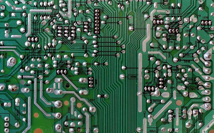
Ⅰ.Causes of film deformation of PCB and solutions
| Causes | (1) Failure of temperature and humidity control |
| (2) Excessive temperature rise of the exposure machine | |
| Solutions | (1) Under normal circumstances, the temperature should be controlled at 22±2°C, and the humidity at 55%±5%RH. |
| (2) Use a cold light source or an exposure machine with a cooling device, and continuously replace backup film. |
Ⅱ.Process methods for correcting film deformation of PCB
1. Under the condition of mastering the operation techniques of the digital programming instrument, first install the film and compare it with the drilling test plate to measure the deformation quantities of its length and width. On the digital programming instrument, adjust the hole positions by lengthening or shortening them according to the deformation quantities.
Use the drilling test plate with adjusted hole positions to align with the deformed film, thereby eliminating the cumbersome work of splicing the film and ensuring the integrity and accuracy of the image. This method is referred to as the “hole position adjustment method.”
2. To address the physical phenomenon where the film changes due to environmental temperature and humidity fluctuations, the film is removed from the sealed bag before copying and hung to dry in the working environment for 4–8 hours. This allows the film to deform before copying, resulting in minimal deformation of the copied film. This method is referred to as the “drying method.”
3. For graphics with simple circuits, wide line widths and spacing, and irregular deformation, the deformed parts of the film can be cut open, reassembled according to the hole positions on the test board, and then copied. This method is called the “cutting and splicing method.”
4. The holes on the test board are enlarged into pads to remove the deformed circuit patterns, ensuring compliance with the minimum ring width technical requirements. This method is called the “pad overlap method.”
5. The “mapping method” involves scaling up the deformed patterns on the film and remapping them for plate making.
6. The “photographic method” involves using a camera to enlarge or reduce the deformed patterns.
BenChuang Electronics produces customized PCB boards, including PCBA and PCB layout services. Contact us and send your specifications.