HomePCB PortfolioDouble sided PCBs

Double sided PCBs

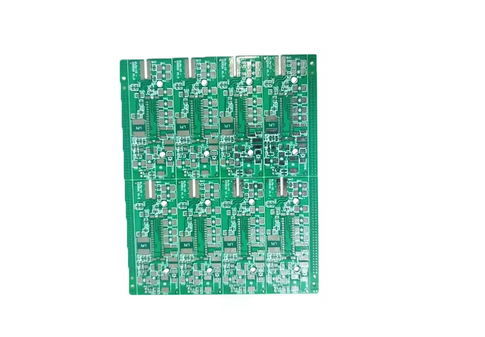
Double sided PCBs are the most widely used products in our product portfolio, with applications ranging from consumer electronics to medical. As technology develops and circuit complexity increases, the demand for Double sided PCBs will decrease. However, this is still our most produced and most reliable product.

FeatureTechnical Specification
Number of Layers2 layers
Technology HighlightsEpoxy glass dielectric materials laminated with copper cladding of varying thicknesses
MaterialsFR-4 standard, FR-4 high performance, FR-4 halogen-free
Copper Weights (Finished)18μm – 210μm, advanced 1050μm / 30oz
Minimum Track and Gap0.10mm / 0.10mm
PCB Thickness0.40mm – 3.2mm
Maximum Dimensions510mm x 650mm
Surface Finishes AvailableHASL (SnPb), LF HASL (SnNiCu), OSP, ENIG, Immersion Tin, Immersion Silver, Electrolytic Gold, Gold Fingers
Minimum Mechanical Drill0.30mm standard, 0.20mm advanced

Double-Sided PCBs: Practical Two-Layer Boards for Balanced Cost and Density

Double-sided PCBs are two-layer circuit boards with copper traces on both top and bottom sides, electrically connected by plated through-holes. They offer far more wiring freedom than single-sided boards while staying simpler and more economical than multilayer designs.

If your layout is getting crowded on one side, or you need both-side components to shrink the board, double-sided PCBs are usually the most cost-effective next step.


1) Double-Sided vs. Single-Sided (Quick Comparison)

ItemDouble-Sided PCBSingle-Sided PCB
Copper layersTwo (top & bottom)One
Routing capacityHigher, easier cross-oversLimited
Component placementBoth sides possibleMostly one side
Layout flexibilityStrongLow
Cost levelModerateLowest

2) What Double-Sided PCBs Help You Achieve

Double-sided boards are chosen when you want:


3) Board Structure (How a Two-Layer PCB Works)

A standard double-sided PCB includes:

This straightforward structure keeps manufacturing stable and helps control cost.


4) When Double-Sided Is the Right Choice

Double-sided PCBs are a strong fit if:


5) DFM Tips That Improve Yield and Assembly

  1. Plan through-holes early
    Hole count and placement decide routing freedom, assembly access, and cost.
  2. Keep soldering clearance safe on both sides
    Especially important if both sides are populated.
  3. Use the bottom layer for stable returns where possible
    Cleaner return paths reduce noise and improve consistency.
  4. Avoid pushing every trace to minimum size
    Keep most nets in stable design windows; reserve tight rules only for critical zones.
  5. Balance copper distribution
    Symmetric copper reduces twist/bow and improves assembly yield.

A short DFM check before release prevents most two-layer problems.


6) Main Cost Drivers (What Changes Price Fast)

Optimizing drilling strategy and layout density usually delivers the biggest savings.


7) RFQ Checklist (Send This for a Fast Quote)

RFQ ItemWhat to provideWhy it matters
Design filesGerber or ODB++Confirms routing, holes, outline
Material intentStandard or special material needsAligns base material route
Copper intentStandard or heavier copper zonesConfirms current/thermal needs
Surface finishENIG / OSP / HASL-LF / otherMatches assembly process
Assembly notesBoth-side parts? special areas?Prevents build surprises
Quantity planPrototype / MPQ / annual volumeSets panel strategy & lead time
Reliability targetsYour test or standard needsDefines validation level

Ready to Start Your Double-Sided PCB Build?

Double-sided PCBs deliver a reliable balance of routing flexibility, stable performance, and cost efficiency. Send your Gerber + assembly notes for a fast DFM review and quotation. Early confirmation of drilling strategy, copper distribution, and finish selection is the shortest path to stable prototypes and smooth mass production.

Talk to an Expert