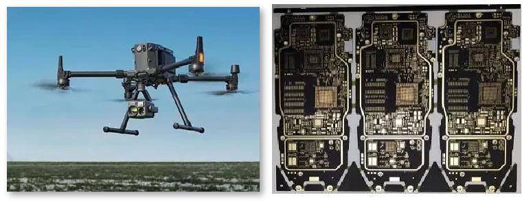
High-End Imaging System Controller PCB | Advanced 12-Layer HDI Solution
Our 12-layer PCB is the perfect solution for high-end imaging systems, designed to deliver top-tier performance and reliability. Engineered for precision, this advanced PCB offers superior durability and signal integrity for demanding imaging applications.
Key Specifications:
- Plate Thickness: 1.0mm – Optimal for high-performance imaging system applications
- Blind Hole Diameter: 0.10mm – Ensures precise and reliable electrical connections
- Minimum Line Width/Line Spacing: 75/75µm – Perfect for intricate circuit designs that require high-density interconnects
- Surface Treatment: Choose from Chemical Gold or Chemical Gold + OSP for enhanced conductivity and protection against corrosion
- Special Process: Level 2 HDI – High-Density Interconnect (HDI) technology enables compact, high-performance designs
Why Choose Our 12-Layer PCB for Imaging Systems?
- Designed for High-End Imaging Systems: Optimized for the performance needs of advanced imaging applications, ensuring top-tier precision and reliability.
- Superior Signal Integrity: The high-density design and fine line width ensure clear and stable signal transmission.
- Advanced Manufacturing: With Level 2 HDI technology, our PCB supports complex, high-performance designs while maintaining compactness and efficiency.
- Durable and Reliable: Built with chemical gold surface treatments, our PCBs offer protection against wear and ensure long-lasting performance in critical imaging applications.
This 12-layer PCB is perfect for high-end imaging systems, where precision, performance, and reliability are crucial. Whether you're working with advanced medical imaging, high-resolution cameras, or other specialized systems, our PCB ensures optimal performance for your application.
Boost your imaging system's efficiency with our high-quality, advanced PCB designs. Contact us today to explore how our HDI PCBs can take your imaging systems to the next level.