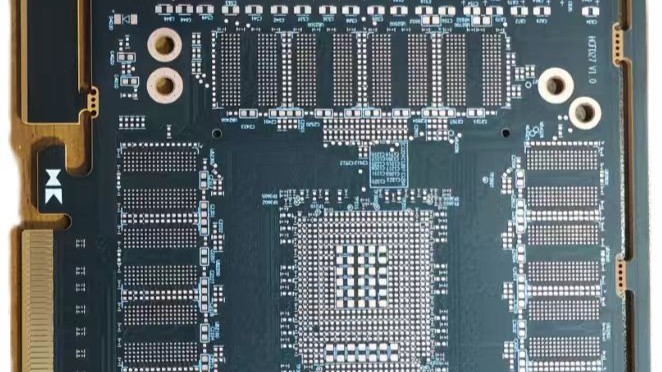
PCB assembly refers to the process of soldering and mounting electronic components onto pre-fabricated printed circuit boards (PCBs). Typically performed using specialized production machinery in batch quantities, the PCB assembly process is commonly referred to as PCBA.

The Process of PCB Assembly
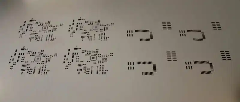
1. Solder Paste Application
First, solder paste (a mixture of fine tin particles and flux) is applied to the board. For this application, most PCB manufacturers use stencils (available in various sizes, shapes, and specifications matching the design). These stencils precisely dispense the correct amount of solder paste onto specific areas of the board.
2. Component Placement
Unlike in the past, this stage of PCB assembly is now fully automated. Component pick-and-place operations—such as placing surface-mount components—were once performed manually but are now executed by robotic pick-and-place machines. These machines precisely position components onto pre-planned areas of the circuit board.
3. Reflow
With solder paste and all surface-mount components in place, curing the paste to the correct specifications is critical for properly bonding the PCB components. This is the relevant part of the PCB assembly process—reflow soldering. To achieve this, the board with solder paste and components is passed through a conveyor belt that traverses an industrial-grade reflow oven. Heaters within the oven melt the solder within the paste. Once melted, the components move again on the conveyor belt and are exposed to a series of cooler heaters. These coolers serve to chill the molten solder and solidify it.
4. Inspection
Following the reflow process, the PCB should undergo inspection to verify its functionality. This stage helps identify poor-quality connections, misplaced components, and short circuits caused by the continuous movement of the board during reflow. PCB manufacturers employ multiple inspection steps—such as manual inspection, automated optical inspection, and X-ray inspection—to verify board functionality, identify substandard solder joints, and uncover potential defects. Following inspection, the assembly team makes critical decisions. Boards with multiple functional errors are typically scrapped, while those with minor defects are sent back for rework.
5. Through-Hole Component Insertion
Certain PCB types require through-hole components alongside standard SMD elements. This stage is dedicated to inserting such components. Plated-through holes are created using PCB components that carry signals from one side of the board to the other. PCB through-hole insertion typically employs manual insertion or wave soldering to achieve results.
6. Final Inspection
This marks the second-level inspection phase. Here, assembled boards undergo functional testing or comprehensive PCB examination to monitor electrical characteristics, including voltage, current, or signal output. Modern manufacturers employ various advanced testing equipment to determine the success or failure of finished boards.
7. Cleaning
Since the soldering process leaves significant flux residue on the PCB, thoroughly cleaning the components is crucial before delivering the final circuit board to the customer. This is achieved by rinsing the PCB in deionized water. Following the cleaning process, compressed air is used to completely dry the board. The PCB assembly is now ready for customer inspection.
BenChuang Electronics produces customized PCB boards. Contact us and send your specifications.