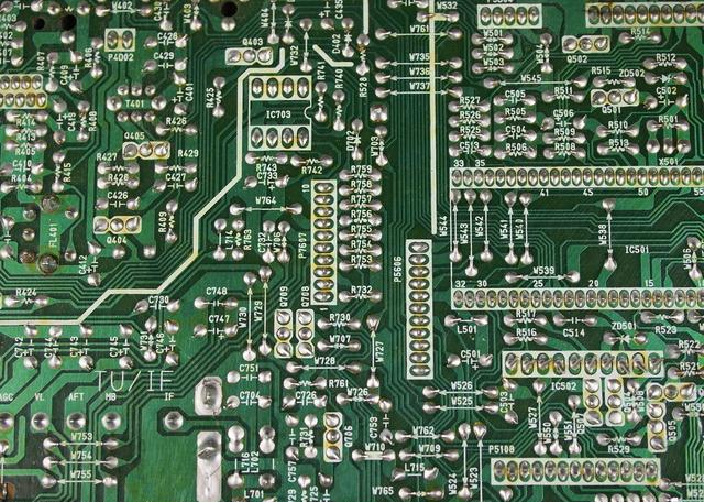
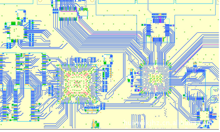
As PCB trace speeds increase, electromagnetic compatibility (EMC) design has become an issue that must be considered. When conducting an EMC analysis of a product and design, the following five important attributes must be considered.
(1) Critical component dimensions
The physical dimensions of the components that generate radiation. RF currents produce electromagnetic fields, which can leak through the enclosure and escape. The length of traces on the PCB directly affects the transmission path of RF currents.
(2) Impedance matching
The impedance of the source and receiver, as well as the transmission impedance between them.

(3) Time characteristics of the interference signal
Whether this is a continuous (periodic signal) event or only exists during specific operational cycles (e.g., a single instance could be a button press or power-on interference, while periodic events could include disk drive operations or network burst transmissions).
(4) Interference signal intensity
How strong is the source energy level, and what is its potential to cause harmful interference?
(5) Frequency characteristics of interference signals
Use a spectrum analyzer to observe waveforms and identify the location of the issue in the spectrum to pinpoint the source of the problem.

Additionally, we should also pay attention to the direction of current flow within circuit components. We know that current flows from high-voltage areas to low-voltage areas, and current always flows through one or more paths in a closed-loop circuit. For applications where interference current direction is measured, modifying PCB traces can prevent them from affecting loads or sensitive circuits. For applications requiring a high-impedance path from the power source to the load, all possible paths through which return current can flow must be considered.
There is also an issue with PCB traces. The impedance of conductors or traces includes resistance R and inductive reactance, and at high frequencies, impedance does not include capacitive reactance. When the trace frequency exceeds 100 kHz, the conductor or trace behaves as an inductor. Wires or traces operating above audio frequencies may act as RF antennas. In EMC specifications, it is not permitted for wires or traces to operate below λ/20 at a specific frequency (the antenna design length equals λ/4 or λ/2 at a specific frequency). If designed carelessly, the trace becomes a highly efficient antenna, making subsequent debugging more challenging.

Finally, let's discuss PCB layout issues.
First, consider the size of the PCB. When the PCB is too large, the increased trace length reduces the system's interference resistance and increases costs, while a PCB that is too small may cause heat dissipation and mutual interference issues.
Second, determine the location of special components (such as clock components). Clock traces should avoid being surrounded by ground planes or placed above or below critical signal traces to prevent interference.
Third, based on circuit functionality, perform overall PCB layout. When placing components, related components should be placed as close together as possible to achieve better interference resistance.


