BenChuang Electronics helps hardware teams move from concept to stable mass production. We integrate precision PCB fabrication with full turnkey assembly, test, and programming, so your RFQ has one accountable owner from stackup to shipment.
Why Engineering Teams Choose Us
- Single partner for PCB + PCBA + test + logistics
- Engineer-first DFM/DFT to prevent late ECOs and rework
- Data-driven quality: AOI, X-ray, and impedance coupons per panel
- Predictable timelines for prototype, pilot, and MP
Core Capabilities (conservative, mass-capable)
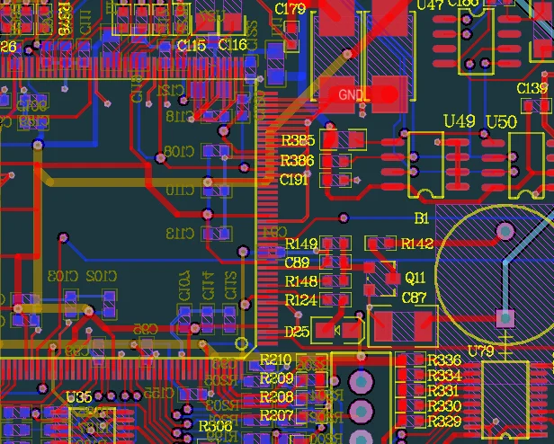
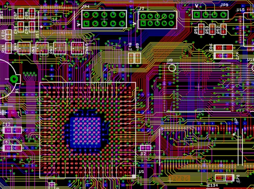
- HDI & Fine Lines: stable 3/3 mil (≈75/75 µm) design rules with LDI imaging and SPC on critical dimensions
- Microvias: 4–8 mil laser microvias; stacked or staggered; via-in-pad with resin/copper fill & cap
- BGA/Routing: dependable escape at 0.35 mm pitch with validated VIP strategies
- Controlled Impedance: typical ±10% on 50 Ω / 90–100 Ω targets; tighter by validation
- Rigid-Flex: PI coverlay, adhesive/adhesive-less options, stiffeners, bend-radius guidance
- Finishes: ENIG / ENEPIG / Immersion Silver / OSP (selected for pitch, bonding, reliability)
OEM & ODM Engagement
OEM (Build-to-Print)
Provide Gerber/ODB++/IPC-2581, BOM with MPNs, PnP/XY, STEP, assembly drawings, and test spec. We manufacture to spec, run 100% E-test, perform X-ray as required, and ship traceable lots.
ODM (Co-Design & Customization)
Share functional targets, interfaces, environment/reliability needs, cost and schedule goals. We propose stackups/materials, advise key parts/alternates, define layout constraints, deliver prototypes → EVT/DVT/PVT, and plan the ramp to mass production.
DFM That Protects Yield and Schedule
- Stackup co-design for impedance and manufacturability
- Rules that work: min line/space, annular ring, VIP keep-outs, back-drill layers agreed up-front
- Panelization tuned for throughput, handling, and low warpage
- Copper balance & thieving to keep boards flat and dimensions stable
Materials & Stackups
- High-TG FR-4 for mainstream HDI and mixed-signal designs
- Low-loss laminates deployed selectively for high-speed/RF layers (hybrid builds)
- Rigid-flex: PI films, coverlay, and stiffeners specified for connectors and wear zones
Deliverables include a manufacturing stackup drawing (foil thicknesses, glass styles, resin content) and a coupon plan for per-panel impedance measurements.
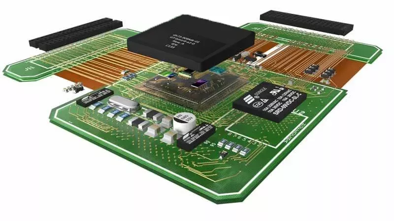
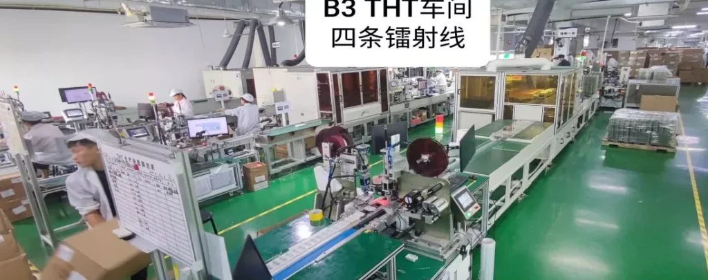
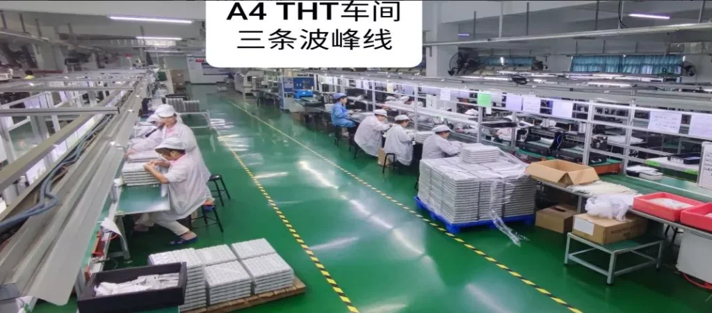
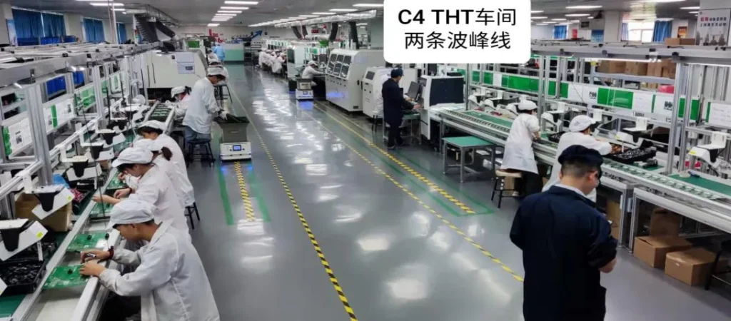
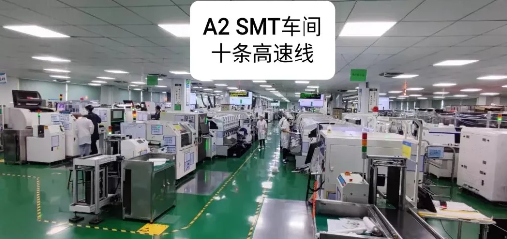
Assembly, Test & Programming
- SMT & selective THD: fine-pitch, µBGA, odd-form; tailored stencils and reflow profiles
- Inspection: AOI inner/outer, BGA X-ray coverage per spec, first-article buy-off
- Test options: flying-probe, ICT, boundary scan, and functional test (FCT) with defined pass/fail limits
- Programming & serialization: HEX/ELF flashing at line speed, unique SN/QR labels, logs returned (CSV)
Traceability, Compliance & Change Control
- Lot-level traceability linking materials, processes, measurements, and test data
- Certificates: RoHS/REACH declarations, COC/COA; automotive PPAP/FAI on request
- Formal ECO flow for deviations and controlled changes
What to Include in Your RFQ (for a Fast, Accurate Quote)
PCB
Layers, size, thickness, materials, copper weight (outer/inner), min line/space, min via (laser/mech), VIP & fill, surface finish, soldermask/legend, impedance targets and tolerance, back-drill, acceptance class (e.g., IPC-6012), test (E-test, impedance coupon), special cleanliness.
PCBA
BOM (with MPNs, alternates policy), centroid/PnP (Top/Bottom), assembly drawings, STEP, solder alloy, stencil (vendor/customer, thickness), reflow constraints, X-ray coverage for BGA, cleaning (no-clean/aqueous), conformal coat/potting, test spec (ICT/boundary scan/FCT), programming image & serialization rules, labeling, acceptance class (IPC-A-610).
Commercial
Quantity breaks, target lead time, Incoterms & destination, packaging (ESD, desiccant, HIC), certificates required, expedite options, and any SLA targets.
Example Use Cases
- 5G/RF module: 10-layer HDI with VIP under fine-pitch BGA, hybrid low-loss stackup, ±10% impedance on coupons
- Automotive controller: traceability with lot records, PPAP/FAI artifacts, thermal cycling sampling on new stackups
- Industrial power board: heavy-copper layers, thermal vias, balanced planes, ICT + FCT coverage
FAQs
Do you support small-batch, high-mix builds?
Yes—staged ramps with shared stencils/fixtures to balance speed and yield.
How tight can impedance tolerance go?
±10% is typical; tighter targets can be validated with specific materials and process windows.
Does via-in-pad increase lead time?
Yes—fill & cap adds processes and curing time. We recommend using VIP where density demands it and standard vias elsewhere.
Can you propose alternates?
With written rules. Key ICs default to “no substitution”; passives/standard parts may follow “form-fit-function equal or higher” criteria.
Get a Turnkey Quote — Upload your Gerber/ODB++ (or PRD for ODM) and tell us your target quantities and timeline. We’ll return a manufacturable plan with clear lead times and yield-aware pricing.