1. Pay attention to the spacing between components
One of the most common issues raised by PCB layout experts is the spacing between components.
Placing two components too close together can cause various problems, potentially requiring redesign and remanufacturing, resulting in time and financial losses.
PCB layout experts typically design layouts with sufficient spacing between component boundaries to mitigate potential issues caused by components being too close together.
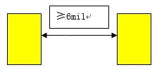
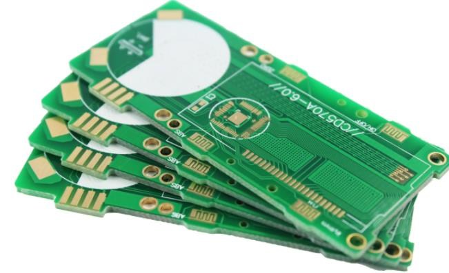
PCB layout engineers must carefully position components to prevent overlapping shapes. In the diagram above, you can see that components are spaced 50 mils apart.
Generally, there are routing and layout rules, such as: the minimum spacing between discrete components like capacitors and resistors should be at least 10 mil, with 30 mil being the preferred spacing. There are also other spacing rules, as shown in the figure below.
2. Select components during the design phase
Experienced PCB layout engineers select components early in the design process to ensure minimal conflicts between the design and actual assembly.
By considering component size and space from the outset, fewer issues arise during PCB assembly.
Generally, smaller components occupy less space on the PCB, so it is worth considering whether component size can be reduced.
3. Separate leaded components from lead-free components
Never mix lead-free components with leaded components. If any component requires lead-free assembly and there are no available traditional leaded solder alternatives, the entire PCB must be assembled lead-free, and all components must comply with lead-free assembly requirements.
Sometimes, the only available package for a specific component is a lead-free BGA. However, there are typically specific requirements in such cases.
Separation plates left between PCBs after routing interfere with connectors extending to that edge. This issue arises when PCB manufacturing and assembly are not closely coordinated.
4. Evenly distribute large components
During layout, distribute large components as evenly as possible across the PCB to achieve optimal thermal distribution during reflow soldering. Ensure that the PCB manufacturer establishes a reflow soldering curve for the reflow soldering process.
5. Do not place surface-mount components too close to the PCB edge
SMD components should be at least 150 mils (3.8 mm) from the edge, especially when using V-grooves.
6. Do not use very small drill bits
Drill holes as small as 6 mils are nearly the smallest mechanical drill holes; they are not recommended unless absolutely necessary. Due to BGA density, it is recommended to use 18.5/8 (18.5 mil pads/8 mil drill holes). Ideally, 22/10 would be good, but BGA does not allow it. (Data is for reference only and may vary depending on specific circumstances)
7. SMD components should be at least 150 mils away from THT components
This facilitates selective wave soldering or wave soldering tray assembly.
8. Proper definition of mounting holes
Typically, mounting holes are defined as tooling holes in the drill diagram with appropriate center points and drill diameters. They are defined with a notch but are not placed on the drill table; instead, they are completed during the less precise routing stage.
9. Clearance around mounting holes
Sufficient clearance must be maintained around mounting holes if other components are present.
BenChuang Electronics produces customized PCB boards. Contact us and send your specifications.