HomePCB PortfolioIC Substrate PCBs

IC Substrate PCBs

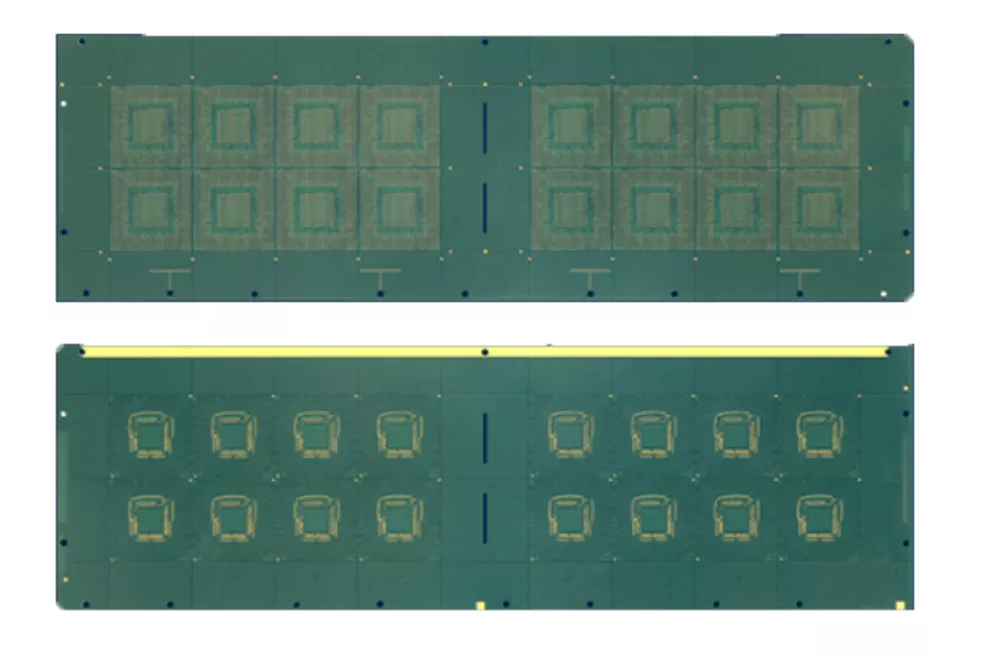
IC Substrate is the chip that makes up the IC bare chip. It is the middle part of the chip package, providing support, heat sink, and protection for the chip, and providing electronic connection between the chip and the PCB. It is a key part in the packaging process, accounting for 35-55% of the packaging process cost.


With the evolution of wafer process technology, the performance requirements for wafer wiring density, transmission rate, signal interference, etc. have increased, which has gradually increased the demand for IC packaging substrates.


SUBFeature
FC-CS2~6 layers
Typical Line Width/Space12/12μm - 25μm/25μm
WB-CSP2~6 layers
Package Size33mm - 2323mm
Thickness0.11mm - 0.56mm
Typical Line Width/Space25/25μm - 40μm/40μm
SiPCompatible with BGA, LGA, Flip Chip, Hybrid solutions
Surface TreatmentSoft Au, ENEPIG, ENIG, SOP, OSP
Heat dissipation performanceFine impedance line width control, excellent heat dissipation performance

IC Substrate PCBs: Built for Advanced IC Packaging

IC substrate PCBs (also called packaging substrates) are the high-density interconnect layer between the silicon die and the system PCB. They enable ultra-fine routing, microvia build-up, stable mechanical support, and controlled electrical/thermal performance for modern packages such as FC-BGA, BGA, CSP, and SiP.

If your design is pushing I/O count, bump pitch, thickness, or high-speed performance, the substrate is the foundation that makes the package manufacturable and reliable.

Free to contact us