If you are designing the next generation of compact, high-power electronic products, you’re probably fighting with the same contradictions every day:
- The enclosure keeps getting thinner.
- The power and functionality keep going up.
- The budget and lead times… do not.
High-performance double-sided PCBs (2-layer PCBs) are one of the most cost-effective ways to balance these pressures. When they are engineered with the right materials, copper thickness and via reliability, they can handle a surprising amount of power and complexity—without forcing you into expensive 4-layer or HDI stacks.
At Shenzhen Benchuang Precision Electronics Co., Ltd. (Benchuang Electronics), we specialize in manufacturing double-sided PCBs for compact and high-power applications used in consumer electronics, industrial control, IoT, and power electronics.
This article will show you when double-sided PCBs are the right choice, what to look for in a manufacturing partner, and how we help overseas engineers move from design files to stable mass production quickly.
Why Double-Sided PCBs Still Matter in a “Multilayer” World
Multilayer and HDI boards get a lot of attention—but for many real projects, a robust double-sided PCB is still the best answer.
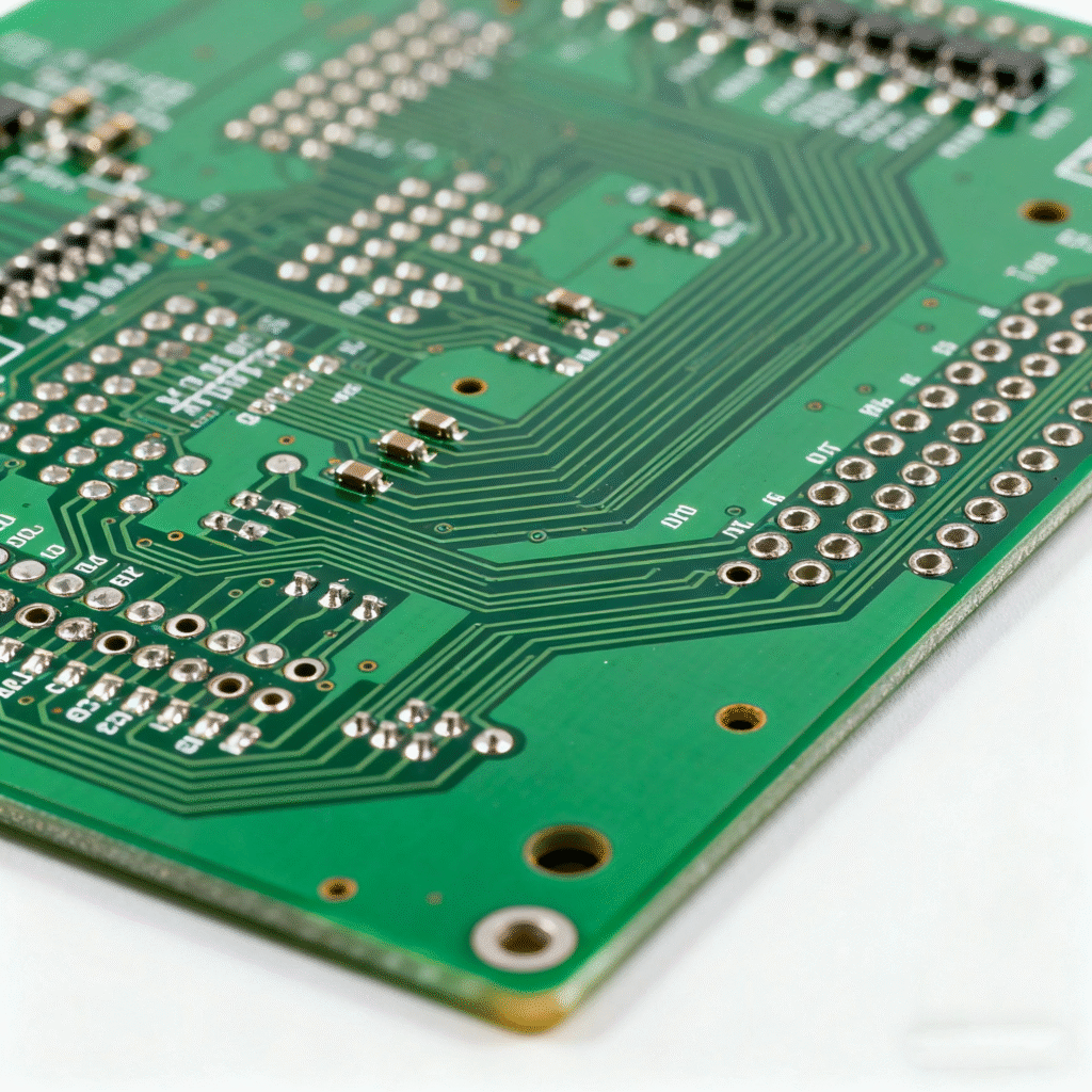
A double-sided PCB uses copper circuits on both the top and bottom layers, connected through plated through-holes (PTHs). This already gives you roughly 50% more component density compared with a single-sided layout, without the cost and complexity of adding more layers.
For product teams, that means:
- Slimmer, lighter devices without sacrificing IO, sensors or power stages
- Simpler stack-up and routing rules than 4-layer or HDI
- Shorter production cycle and lower unit cost – many projects can be produced faster and cheaper than equivalent 4-layer solutions
If your design is pushing size, power or reliability, the key is not “more layers at any cost” but better engineering of the two layers you already have.
What Makes a “High-Performance” Double-Sided PCB?
Not all 2-layer boards are created equal. For compact, high-power and high-frequency applications, material and process choices make the difference between “works in the lab” and “survives in the field”.
At Benchuang Electronics, our double-sided PCBs are built around the following core specifications and optional upgrades:
1. Base Materials for Reliability & Frequency
- Standard: FR-4 (flame retardant)
- High-performance options:
- FR-4 High Tg (170 °C+) for high-frequency / high-temperature designs
- Aluminum substrate or high-frequency materials (e.g. Rogers) for special power or RF modules
High-Tg FR-4 and stable dielectric properties help reduce signal attenuation and crosstalk, which is critical for 5G modules, Wi-Fi 6 routers, and high-speed digital buses.
2. Copper & Board Thickness for Power Density
- Standard copper: 1 oz (35 µm) / 2 oz (70 µm)
- Custom range: 0.5–6 oz for high-current designs
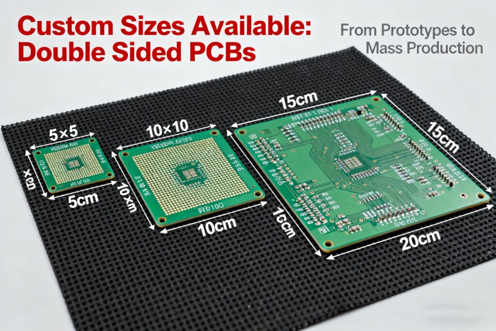
- Standard board thickness: 0.8–2.0 mm
- Custom range: 0.4–6.0 mm
For charging piles, LED drivers, inverters and other power boards, we often recommend 2 oz or thicker copper on double-sided PCBs to safely handle higher current while keeping the design in a cost-effective two-layer stack.
3. Surface Finishes & Via Quality for Stable Performance
- Surface finishes:
- Standard: HASL, ENIG (immersion gold)
- Optional: OSP, immersion silver, ENEPIG
- Via plating thickness: typically ≥ 20 µm via copper thickness for reliable current transmission through PTHs
Combining high-Tg FR-4 with ENIG is particularly suitable for fine-pitch ICs, BGAs and high-speed signals, where flatness and oxidation resistance are essential.
4. Solder Mask & Environmental Resistance
We use scratch-resistant, wear-resistant solder mask inks with excellent salt spray resistance, and we can support IP65-grade waterproof packaging for boards used in dusty or humid environments. The PCBs meet UL 94 V-0 flame retardant certification, giving extra safety margin for demanding industrial and automotive scenarios.
Color options include green (standard), black, blue, white and matte green to match your product line or end-customer requirements.
Compact Designs: Where Our Double-Sided PCBs Are Used
Because of their balance of performance and cost, our double-sided PCBs are widely used across several industries. Here are a few representative scenarios from our production experience.
Consumer Electronics – Thinner, Smarter Devices
Typical applications:
- Smartphone motherboards and power boards
- Tablet and laptop power management boards
- TWS earphone charging cases
- Wearable sensor modules (watches, fitness bands, AR/VR peripherals)
Example:
By optimizing PCB layout, copper distribution and component placement on double-sided boards, a mobile device customer achieved both a noticeable increase in battery capacity and a slimmer device body—without moving to a more expensive multilayer stack.
Industrial Control – Stable Under Harsh Conditions
Typical applications:
- PLC mainboards
- Servo motor driver boards
- Sensor interface boards for automated production lines
Example:
For an automotive parts manufacturer, we customized high-temperature resistant double-sided PCBs capable of continuous operation at elevated temperatures in engine compartment environments.
IoT & Smart Devices – Low Power, Long Life
Typical applications:
- Smart door locks
- Environmental monitoring sensors (temperature, humidity, PM2.5)
- Smart home gateway boards
Example:
We supported an agricultural IoT company with low-power double-sided PCBs and optimized copper and trace routing. The result: their field sensors’ battery life increased significantly, reducing maintenance and replacement costs.
Power Electronics – High Current on a Budget
Typical applications:
- LED driver power boards
- EV charging pile control boards
- Inverter circuit boards
Example:
A new-energy customer needed to transmit high current in a compact board area. We delivered thick-copper double-sided PCBs that met the current requirements while keeping the solution in a cost-effective 2-layer configuration.
When to Choose Double-Sided PCBs Over 4-Layer or HDI
From our experience with overseas engineers and buyers, double-sided PCBs are usually the best choice when:
- Your mechanical design demands a slim and compact board, but not ultra-high layer density
- You need to balance performance with cost in small to medium batches
- Your power or frequency requirements can be handled by proper copper thickness, via design, and material selection
- You want shorter production cycles for faster prototype validation and market launch
If your current design is on 4 layers purely for “safety” but not because it truly needs the extra routing capacity, it is often worth sending us the Gerber files for a DFM (Design for Manufacturability) review. In many cases, we can recommend a robust double-sided alternative that meets your electrical and thermal requirements and lowers your BOM.
How We Work With You: From Gerber to Mass Production
To help overseas customers move quickly from idea to product, we designed a simple 3-step process around our double-sided PCB line:
Step 1 – Send Design Files
You provide:
- Gerber files / ODB++
- Basic requirements (target application, volume, special materials or finishes)
Step 2 – DFM & Optimization
Our engineering team performs a DFM analysis focusing on:
- Via design and hole sizes
- Trace width / spacing vs. current
- Heat dissipation and copper balancing
- Solder mask opening and manufacturability
We share suggestions for layout optimization, heat dissipation, and reliability improvement—free of charge.
Step 3 – Rapid Prototyping & Mass Production
Once you confirm the solution:
- Prototype samples can be produced quickly
- Mass production delivery can be arranged within a short lead time, depending on order size and process combination
Throughout the project, our engineers are available online to support technical questions, design adjustments or urgent schedule changes.
Looking for a Reliable Double-Sided PCB Partner in China?
If you are:
- Migrating an existing product from 4-layer to 2-layer to control cost
- Designing a new compact device that must stay cool and reliable
- Searching for a PCB factory that can truly understand your Gerber files and suggest improvements—not just “build to print”
…then our double-sided PCB line is designed for you.
Benchuang Electronics is based in Shenzhen, Guangdong, with a complete PCB manufacturing and quality-control system serving global OEM/ODM customers.
Start Your Double-Sided PCB Project Today
You don’t need a complicated process to get started:
- Email your Gerber files or design drawings
- Tell us your target application, volume and any special requirements
- Receive a free quotation + DFM suggestions
📧 Email: William@bcpcbsz.com
📱 WhatsApp: +86 17724684094
If you are ready to improve space utilization, signal integrity and reliability while staying within budget, send us your files today. Our team will help you turn your PCB design into a stable, manufacturable solution—so you can focus on what matters most: building competitive, high-performance products for your market.