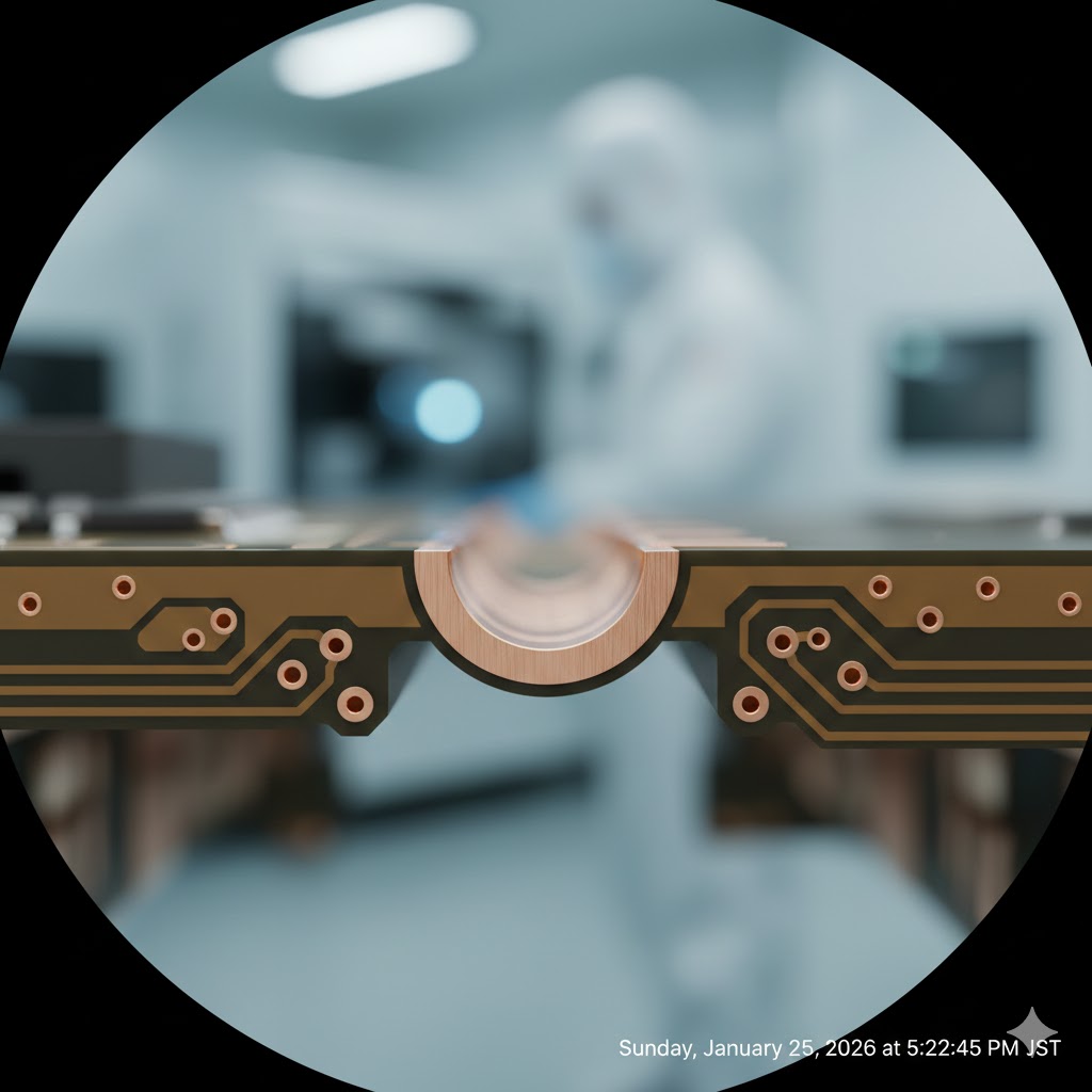
Engineered for seamless system integration, our Module PCBs feature precision Half-Via (Castellated Hole) technology with a $\pm 0.05\text{mm}$ tolerance. Optimized for IoT and RF applications, our manufacturing process ensures burr-free edges and $\pm 5\%$ impedance control to maintain signal integrity across ultra-thin substrates. From ISO Class 5 cleanrooms to IATF 16949-certified mass production, we deliver the reliability required for high-yield SMT assembly.
CORE ADVANTAGES FOR POWER & CONTROL
[1] DUAL-FUNCTION INTEGRATION We master the art of integrating heavy copper traces (for power delivery) with fine-pitch HDI routing (for MCU/FPGA control). This reduces module size and eliminates interconnection bottlenecks.
[2] ADVANCED THERMAL MANAGEMENT Power modules generate heat. We utilize Thermal Vias, Metal Core (MCPCB) inserts, and high-Tg materials to ensure your control logic remains stable even under high-load thermal stress.
[3] SUPERIOR SIGNAL INTEGRITY Our high-density routing minimizes EMI (Electromagnetic Interference) between power switching circuits and sensitive control signals, ensuring zero-glitch performance in industrial environments.
[4] RUGGEDIZED FOR EXTREME CONDITIONS Built to withstand vibration, moisture, and temperature fluctuations. Our boards serve Aerospace, Medical, and Automotive sectors where failure is not an option.
⚙️ APPLICATIONS
INDUSTRIAL AUTOMATION: PLC controllers, Servo drives, and Robotic arm modules.
EV & ENERGY: On-board chargers (OBC), Battery Management Systems (BMS), and Inverters.
RENEWABLE ENERGY: Solar power optimizers and wind turbine pitch controllers.
AEROSPACE: Power distribution units (PDU) and flight control systems.
MEDICAL DEVICES: High-power imaging systems and precision surgical robotics.