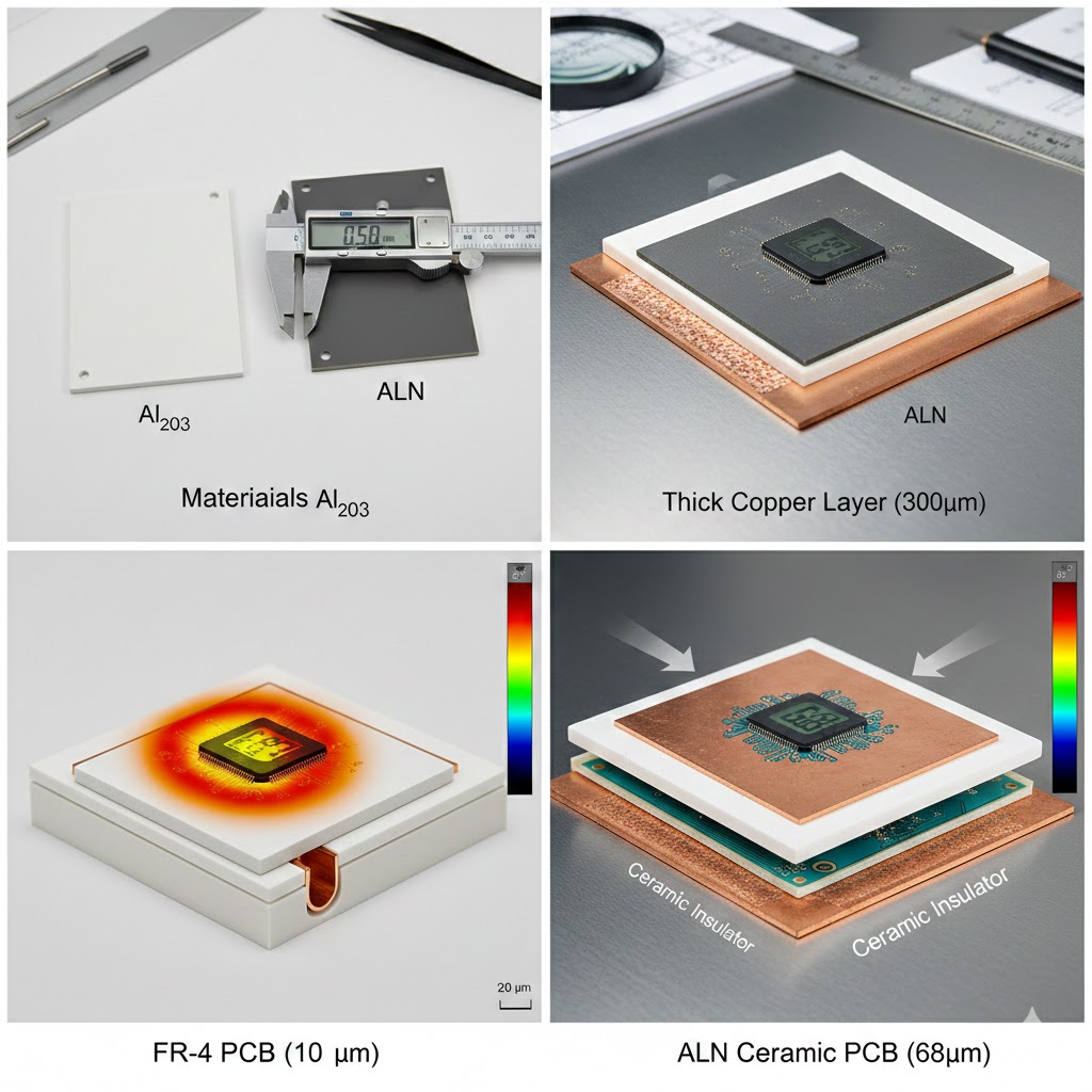
Engineered for most demanding thermal and power environments. Benchuang provides industry-leading Ceramic PCBs using Alumina (Al2O3) and Aluminum Nitride (AlN). We bridge the gap between extreme power and stable performance.
1-20 Layers Multilayer Capability
Up to 230 W/m.K Thermal Conductivity
7-15 Days Rapid Turnaround
19 Years of Manufacturing Excellence (Since 2007)
🌟 PRODUCT OVERVIEW
Engineered for most demanding thermal and power environments. Benchuang provides industry-leading Ceramic PCBs using Alumina (Al2O3) and Aluminum Nitride (AlN). We bridge the gap between extreme power and stable performance.
1-20 Layers Multilayer Capability
Up to 230 W/m.K Thermal Conductivity
7-15 Days Rapid Turnaround
19 Years of Manufacturing Excellence (Since 2007)
💎 CORE ADVANTAGES
[1] UNMATCHED THERMAL MANAGEMENT Ceramic substrates offer heat dissipation 10-20x higher than traditional FR-4. Essential for high-power modules where heat is the enemy.
[2] PRECISION CTE MATCHING The Coefficient of Thermal Expansion (CTE) is perfectly tuned to silicon chips, preventing solder joint fatigue and ensuring long-term module stability.
[3] SUPERIOR DIELECTRIC PERFORMANCE Ultra-low dielectric constant and loss tangent. Ideal for 5G, RF, and High-Frequency signal integrity.
[4] EXTREME DURABILITY
Temperature Resistant: Stable performance up to 400°C+.
Corrosion Proof: Chemically inert and moisture resistant.
High Voltage: Naturally superior electrical insulation.
🛰️ APPLICATIONS
AUTOMOTIVE: IGBT Modules, EV Inverters, ADAS Sensors.