BenChuang Electronics manufactures HDI and ultra-fine line PCB for telecom, automotive, medical, industrial control and semiconductor equipment. We support prototype, pilot and mass production with stable processes including laser drilling, LDI imaging, sequential lamination, via-in-pad, copper filling and controlled impedance builds.
1) Fine Line / Space: What We Hold Stably
Stable production rules (conservative, mass-capable):
- Min line/space: 3/3 mil (≈75/75 µm) across qualified materials
- Typical copper: 1/2–1 oz outer layers; 1/3–1/2 oz inner layers for fine lines
- Registration: artwork-to-soldermask alignment tightly controlled with LDI and optical fiducials
- BGA escape: reliable routing at 0.35 mm pitch with appropriate pad/via strategy
How we ensure stability
- LDI for uniform exposure; fine-grain resist to reduce undercut
- Etch compensation per panel zone; copper balancing on opposing layers
- SPC on critical dimensions (line width, annular ring) with periodic micro-sections
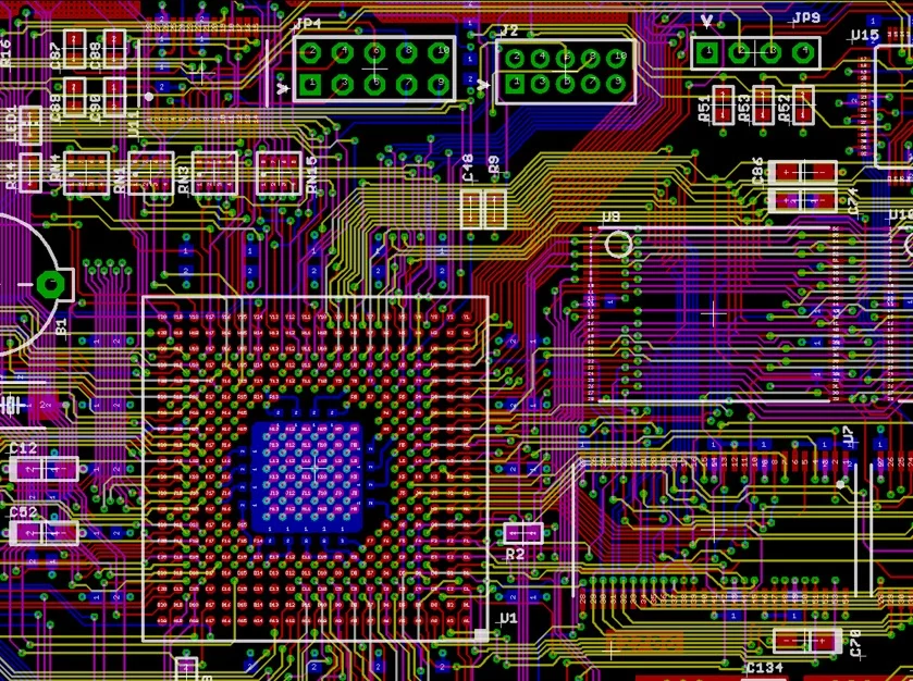
2) Microvia Structures: Size, Fill, Stack Strategy
Capabilities
- Laser microvia diameter: 4–8 mil (≈0.10–0.20 mm), dielectric thickness matched to keep aspect ratio ≤ 0.8
- Blind/buried/stacked: staggered or stacked uVias; stacked height qualified case-by-case
- Via-in-pad (VIP): resin-filled & capped or copper-filled for flat pads and reliable assembly
- Back-drill: available to remove stubs on high-speed nets
Process controls
- Laser energy calibration by dielectric set; coupon cross-sections each lot
- Fill density & void inspection; flatness control after fill-and-cap
- Thermal stress qualification for stacked structures on new stackups
3) Controlled Impedance: Design-to-Measurement Loop
Design support
- Pre-layout guidance on target impedance (e.g., 50 Ω/90 Ω/100 Ω single-ended/differential)
- Material and foil selection (low-loss where needed), glass style choice, and resin content targets
- Verified field-solver stackups (core vs. prepreg, RCC where applicable)
Manufacturing & validation
- Impedance coupon on every panel; TDR measurement logged per lot
- Typical tolerance: ±10% (tighter on request with matched material/foil/process windows)
- Copper roughness and etch-factor modeled against final thickness to hit target Z
4) Materials & Stackups (Examples We Run Frequently)
- FR-4 systems: High-TG FR-4 for mainstream HDI; RCC options for finer lines
- Low-loss options: For RF/high-speed layers, hybrid builds can be evaluated
- Surface finishes: ENIG / ENEPIG / Imm-Silver / OSP; finish chosen by pitch, wire-bonding or corrosion requirements
- Thermal design: Copper balancing, thieving patterns and via-in-pad with fill to mitigate warpage on large panels
We provide a manufacturing stackup drawing before CAM release, including foil thickness, dielectric thickness, glass styles and target impedance tables.
5) Quality & Reliability Controls
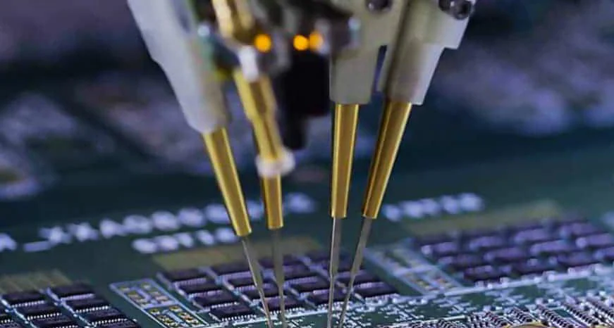
- Inspection: 100% AOI on inner/outer layers; X-ray on BGA/VIP; flying-probe/ICT based on build stage
- Reliability: Thermal cycling/thermal shock sampling for new stackups; solderability checks per lot
- Traceability: Lot-level process records linked to coupon data and materials
- KPIs (monitored internally): first-pass yield, on-time delivery and field RMA rate; corrective actions tracked to closure
6) Practical DFM Rules (Engineer-Friendly)
- Lines/spaces: keep critical nets at ≥ 3/3 mil unless pre-approved; relax on non-critical nets to improve yield
- Annular ring: design for ≥ 3 mil on laser vias; discuss pad-stack if going tighter
- Dielectric: maintain microvia dielectric per layer pair to keep aspect ratio ≤ 0.8
- Impedance: avoid mixing glass styles across mirrored layers; confirm copper distribution to reduce skew
- VIP: reserve keep-out around VIP lands; we’ll advise minimum mask clearance and cap thickness
We share a short, one-page HDI DFM checklist during RFQ so layout teams can lock rules early and avoid late-stage ECOs.
7) Case Snapshot (Typical HDI Build)
- Application: 5G radio module, mixed-signal and high-speed
- Stack: 10-layer HDI with L1–L2/L9–L10 microvias, staggered to L3/L8
- Targets: 100 Ω diff (high-speed pairs), 50 Ω single-ended (RF)
- Tactics: low-loss cores for high-speed layers, copper balancing on power planes, VIP under fine-pitch BGA
- Outcome: coupons measured within ±8–9% of target; assembly coplanarity met on VIP pads; no warpage issue after reflow profiling
8) What to Include in Your RFQ (Speeds Up CAM & Quoting)
- Gerber/ODB++, netlist (if available), preliminary stackup or target impedance
- Layer count, board thickness, min line/space, min via (laser/mechanical)
- VIP/copper-fill needs, surface finish, copper weights per layer
- Soldermask color/gloss, legend, panelization preference
- Test strategy (flying-probe/ICT), special cleanliness or ionic requirements
- Prototype vs. mass production lead-time expectations
Why BenChuang
Stable fine-line yields, disciplined microvia processes, and a closed impedance loop from design through coupon measurement—that’s what makes HDI builds repeatable here. For your next NPI or mass build, send us your stackup idea and target impedance; we’ll return a manufacturable proposal with DFM notes and coupon plan.