Move beyond the limits of traditional HDI. Our SLP (Substrate-Like PCB) leverages mSAP technology to deliver $15/15\mu m$ precision, enabling a 30% reduction in board size for 5G, wearables, and SiP modules. From ISO Class 5 cleanrooms to IATF 16949-compliant mass production, we provide the technical certainty your next-gen hardware demands.
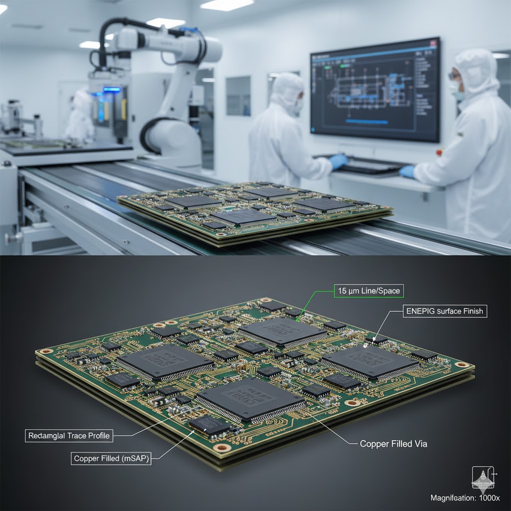
Benchuang’s SLP (Substrate-Like PCB) utilizes the mSAP (modified Semi-Additive Process) to achieve finer traces and higher reliability, mimicking the performance of an IC substrate on a larger board scale.
mSAP Technology for Squared Trace Cross-Sections
Ultra-Fine Line/Space: Down to 25μm/25μm
19 Years of Precision Engineering (Est. 2007)
Rapid Delivery: Prototyping to Mass Production in 7-15 Days
🔥 CORE ADVANTAGES OF BENCHUANG SLP
[1] REVOLUTIONARY mSAP PROCESS Unlike traditional subtractive etching, our mSAP process creates traces with vertical walls and precise geometries. This ensures superior impedance control and high signal integrity for high-frequency 5G applications.
[2] EXTREME SPACE OPTIMIZATION SLP reduces the area required for routing by 30-50% compared to Any-layer HDI. This frees up critical internal space for larger batteries, more sensors, or thinner device profiles.
[3] HIGH-DENSITY INTERCONNECTIVITY Supporting massive layer counts (up to 20 layers) with stacked microvias and ultra-thin cores. We enable the most complex AI and mobile chipsets to communicate with zero latency.
[4] AEROSPACE-GRADE RELIABILITY Based in Shenzhen, our facility integrates 19 years of experience serving Aerospace, Medical, and Automotive sectors, ensuring every SLP meets rigorous IPC Class 3 standards.
📱 APPLICATIONS
NEXT-GEN SMARTPHONES: Essential for 5G/6G mainboards and RF modules.
WEARABLE TECH: Smartwatches and AR/VR glasses where every millimeter counts.
AI & COMPUTING: Edge AI modules and compact high-performance computing (HPC).
MEDICAL MINIATURIZATION: Implantable devices and handheld diagnostic tools.
AUTOMOTIVE ADAS: High-density processing units for autonomous driving.