BenChuang Electronics PCB Factory: Quality Control in High-Density Interconnect PCB Manufacturing
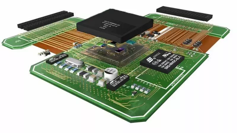
Part 1: A Close Look at Common HDI PCB Defects
1.1 Micro-via Filling Issues
In HDI PCB manufacturing, the quality of micro-via filling has an immediate impact on signal integrity and long-term reliability. If the laser energy is too low or the drill speed is too high, the hole wall becomes rough and copper adhesion suffers. At BenChuang Electronics, we use fully automatic laser drill lines with closed-loop energy control; this keeps drilled-hole diameter tolerance within ±2 µm and pushes micro-via filling rates to 99.8%.
1.2 Fine-Line Opens / Shorts
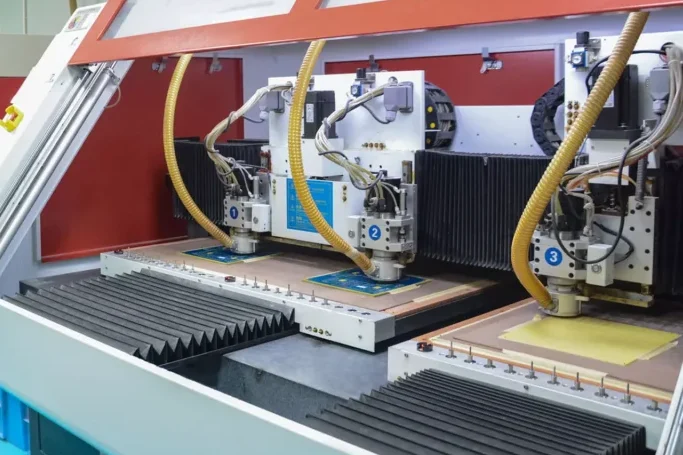
When line/space drops to 3 mil/3 mil, photoresist exposure accuracy decides the yield. Our Class 1000 clean room employs laser-direct-imaging (LDI) technology to remove photo-tool expansion errors, and we follow that with automatic developing lines. Together, these steps hold etch uniformity to ±1 µm and lift fine-line yield on our 50k m²/month line to 99.5%.
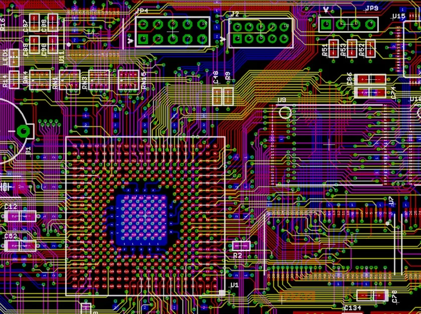
1.3 Layer-to-Layer Mis-registration
On an eight-layer HDI build, cumulative mis-registration can exceed 50 µm. We run optical alignment on every lamination cycle and use high-precision pinned tooling. The result is ≤25 µm layer-to-layer shift—tight enough for 0.3 mm-pitch BGA pads.
Part 2: Design-for-Manufacturing (DFM) Guidelines for HDI PCB Boards
2.1 Cost-Control at the Design Stage
Material choice drives both cost and performance. For 5G hardware, we often recommend Panasonic M6 (Df 0.002 @10 GHz); it cuts insertion loss by 30% versus standard FR-4. BenChuang's free DFM review—stack-up optimisation, impedance calculation, and material advice—saved customers an average of 18% on material cost in 2024. Every enquiry receives a full engineering report within 24 hours.
2.2 Key DFM Checkpoints
IPC-2226 advises a minimum laser-drilled hole of 0.1 mm and an aspect ratio ≤1:1. For 0.65 mm-pitch BGAs, we suggest via-in-pad with resin plugging and plated-over technology. As an IPC-member shop we work to IPC-6012D; our CAM engineers hold IPC-D-300G certification and translate design data with 99.9% accuracy.
2.3 Standardising Special Processes
Buried via depth is held to ±5 µm by auto-focus laser drills. Where PTFE substrates are needed for RF performance, plasma treatment raises hole-wall roughness above 2 µm to guarantee copper adhesion. Thanks to detailed SOPs, first-pass yield on special-flow boards runs at 98%+.
Part 3: Process Quality-Control System
3.1 Incoming Inspection & Traceability
Every laminate lot is verified for Tg (DSC), CTE (TMA), and Dk (SPDR). Long-term agreements with Rogers, Isola, and Panasonic give us priority supply and price stability. Each panel receives a unique ID; our MES logs all parameters, so any issue can be traced and contained within two hours.
3.2 SPC at Critical Operations
Laser drill CPK targets are ≥1.67; closed-loop power feedback keeps 0.1 mm holes within ±0.5 mil. In plating, automatic additive controllers hold copper uniformity to ±1 µm. Real-time data are collected on every panel; critical dimensions are checked 100%.
3.3 Final Test & Reliability Verification
Flying-probe testers verify nets down to 5 µm accuracy. For automotive and medical customers, we run IST testing per IPC-TM-650. Our in-house CNAS lab issues more than 2,000 reliability reports a year, complete with X-ray, micro-section, and SEM data.
Part 4: Cost Optimisation & On-Time Delivery
4.1 Understanding HDI Cost Structure
Material typically accounts for 45-55% of total cost; high-frequency laminates such as Rogers RO4350B can cost ten times standard FR-4. Joint value-engineering with customers cut premium material usage 25% for one telecom program and saved US$1.2M annually. Our scale purchasing keeps major material costs 8-12% below the industry average.
4.2 Fast-Turn Capability
Standard HDI lead-time is 6–8 days; 48-hour expedite is available for prototypes. Flexible planning cuts change-over time to 30 minutes; three-shift operation secures 50k m² monthly capacity. On-time delivery hit 96.8% in 2024, earning "preferred supplier" status from Huawei, BYD, and other tier-one customers.
4.3 High-Yield Mass Production
Six-sigma tools keep key-process defect rates below 3.4 ppm. Overall HDI yield reached 98.7% last year—3.2 points above the industry average. Customer surveys show 96.5% satisfaction and an 89% repeat-order rate.
Why Choose BenChuang Electronics as Your HDI PCB Manufacturing Partner?
- 18 years focused on HDI technology
- 50k m² monthly capacity with 98.7% yield
- 48-hour prototype turn available
- Free DFM review and 24-hour engineering support
- One-stop turnkey PCBA services from PCB to final assembly
Contact our engineering team today for a free DFM report. We look forward to becoming your reliable PCB supplier in China and supporting your next high-density interconnect project from design to delivery.