Drone PCB: Engineering High-Performance Reliability for the Next Generation of Flight
The Drone PCB is the central nervous system of any UAV. As industrial demands scale, standard boards hit a "performance wall" of weight and vibration failure. We provide high-performance Drone PCB solutions—engineered with heavy copper and ultra-light HDI—to bridge the gap between ambitious prototypes and flight-ready, market-leading platforms.
1. Defining "High-Performance" Through Engineering Metrics
In the drone industry, "High Performance" isn't a marketing buzzword; it is a set of quantifiable survivability metrics. We define it through four critical pillars:
Extreme Power Density (Current Handling)
Modern drones require massive instantaneous power during high-G maneuvers or heavy-lift take-offs.
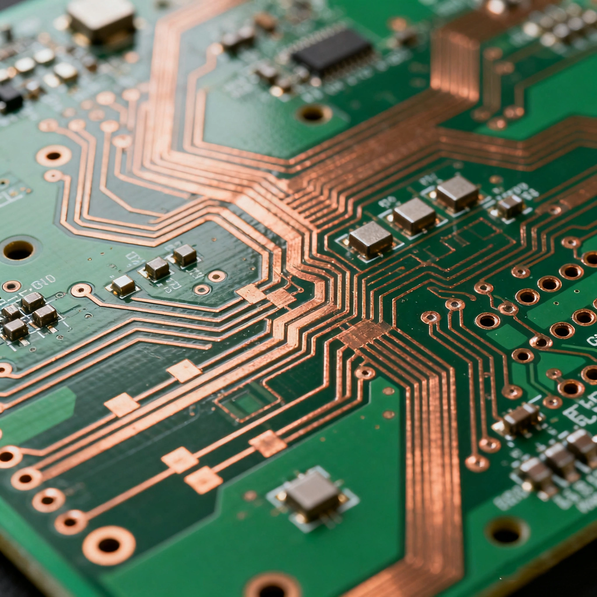
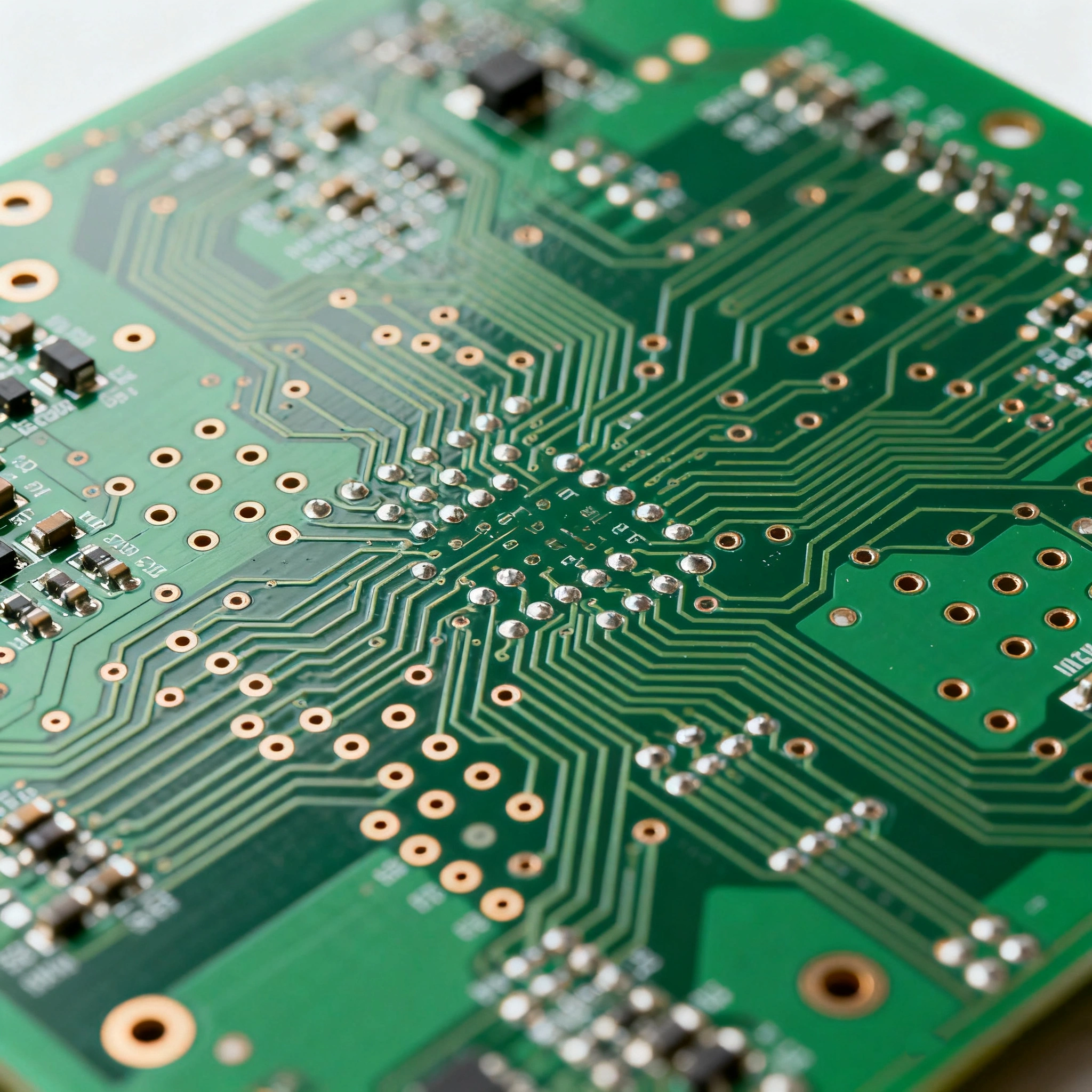
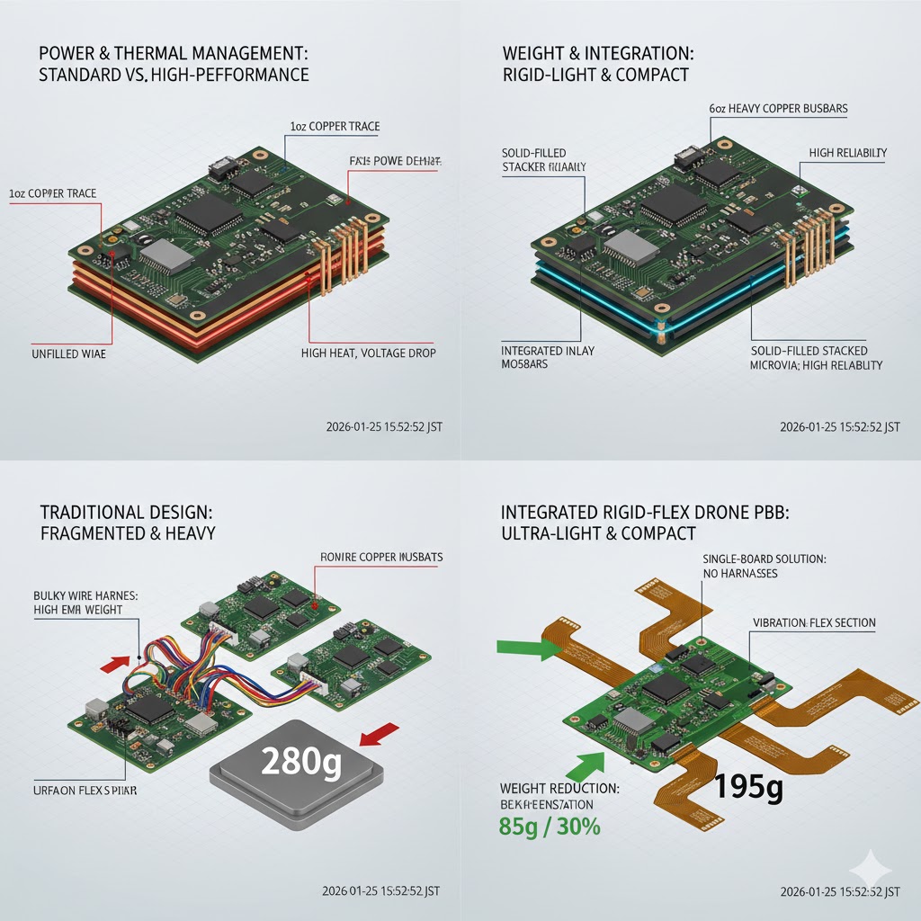
The Spec: Support for 120A continuous current and 200A burst surges (10s) on a single substrate.
The Tech: Utilizing Heavy Copper (up to 6oz) and embedded busbars to eliminate voltage drops, ensuring your ESCs (Electronic Speed Controllers) receive stable power during aggressive climbs.
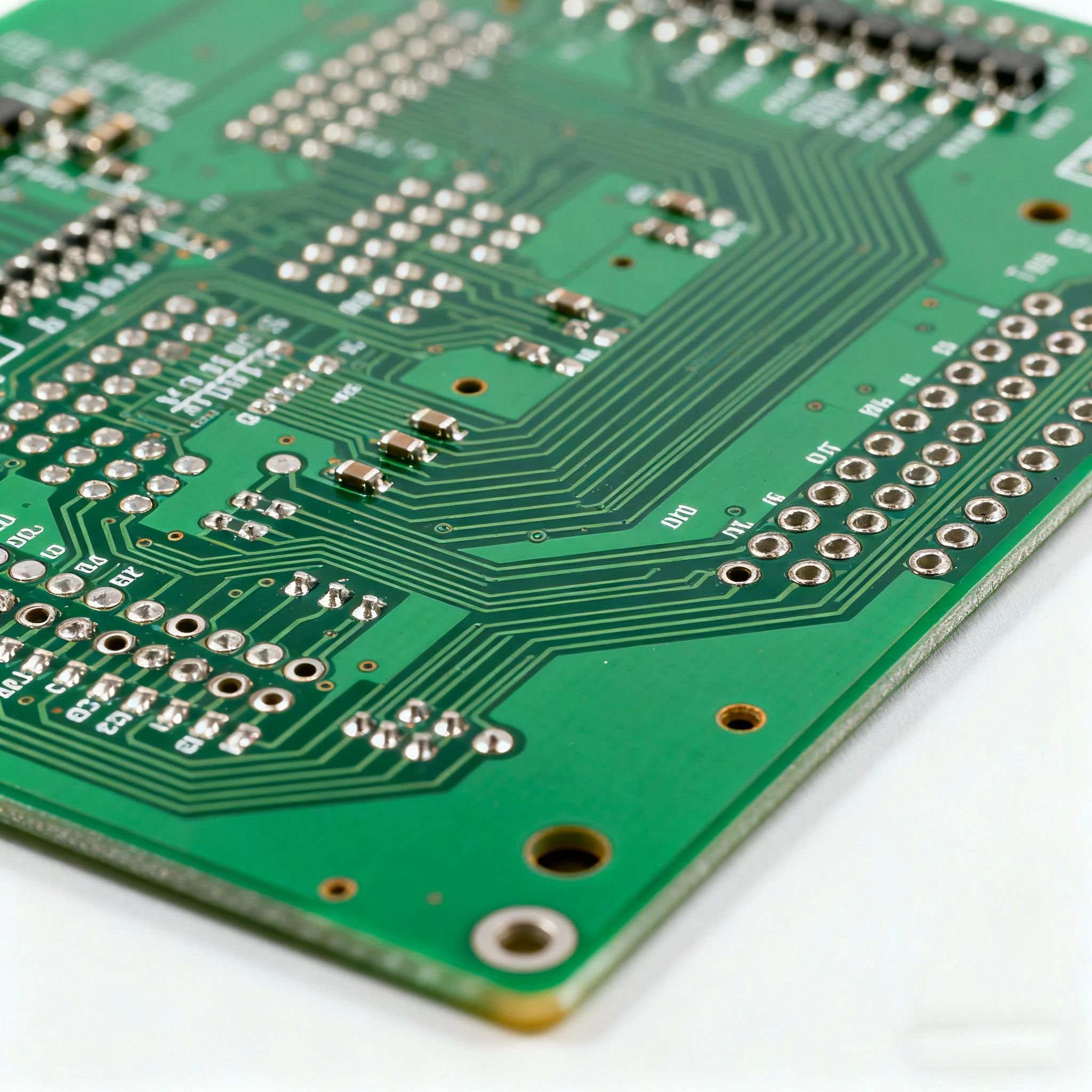
Vibration-Resistant Interconnects (IPC Class 3)
The high-KV motors used in modern UAVs create intense harmonic resonance that can shatter standard solder joints and via structures.
The Spec: Zero failure after 100+ hours of high-G vibration testing.
The Tech: We implement Solid-Filled Stacked Microvias and high-toughness High-Tg resins to prevent via-cracking caused by structural harmonics and frame resonance.
Strategic Weight Reduction
Every gram of "dead weight" on a PCB is a gram removed from your battery capacity or sensor payload.
The Spec: Achieving a 15-25% reduction in board weight compared to standard 1.6mm FR-4.
The Tech: Using Ultra-Thin HDI (0.4mm - 0.6mm core) and Rigid-Flex integration. By eliminating bulky wire harnesses and heavy connectors, we free up critical mass for mission-specific equipment.
EMI Isolation for Sensitive Sensors
High-power ESC switching noise is the enemy of GPS locks and IMU stability.
The Spec: A measured 12dB improvement in Signal-to-Noise Ratio (SNR) for critical navigation data.
The Tech: Precision layer stackups that act as an internal "Faraday Cage," isolating high-frequency switching noise from the sensitive flight controller logic.
2. Technical Comparison: Standard vs. High-Performance Drone PCB
High-Perf Metric
Engineering Specification
The Flight Advantage
Current Capacity
120A+ Continuous / 200A Burst
Prevents board burnout under heavy lift
Copper Weight
3oz - 6oz (Inner & Outer)
Ultra-low resistance & minimal heat
Via Reliability
Solid-Filled Stacked Microvias
Survives 15,000+ RPM motor resonance
Substrate Thickness
0.4mm - 0.8mm (Thin-Core)
Increases flight time by 10-15%
Impedance Control
±5% Precision
Crystal-clear 4K/6K video transmission
3. Case Study: Extending Endurance by 25%
The Challenge: An industrial inspection drone was suffering from "Fly-Away" incidents caused by GPS signal interference and limited flight times due to heavy internal wiring.
The Solution: We replaced a complex 4-board system with a single Integrated Rigid-Flex Drone PCB.
The Result: By consolidating the PDB, ESC signals, and Flight Controller into one board, we slashed 85g of weight and eliminated EMI noise. The aircraft achieved a 25% increase in mission duration and maintained a rock-solid GPS lock in high-interference urban environments.
4. Why Reliability is Your Best ROI
In the UAV sector, "High Performance" equals "Lower Liability." A failure in the Drone PCB results in a total loss of the aircraft and potential damage to ground assets. By specifying high-performance metrics, you aren't just buying a circuit board—you are investing in flight insurance.
Ready to Elevate Your Flight Hardware?
Don't let standard PCB limitations ground your innovation. Contact our engineering team today for a comprehensive DFM Review and a custom Drone PCB quote tailored for high-performance mission profiles.
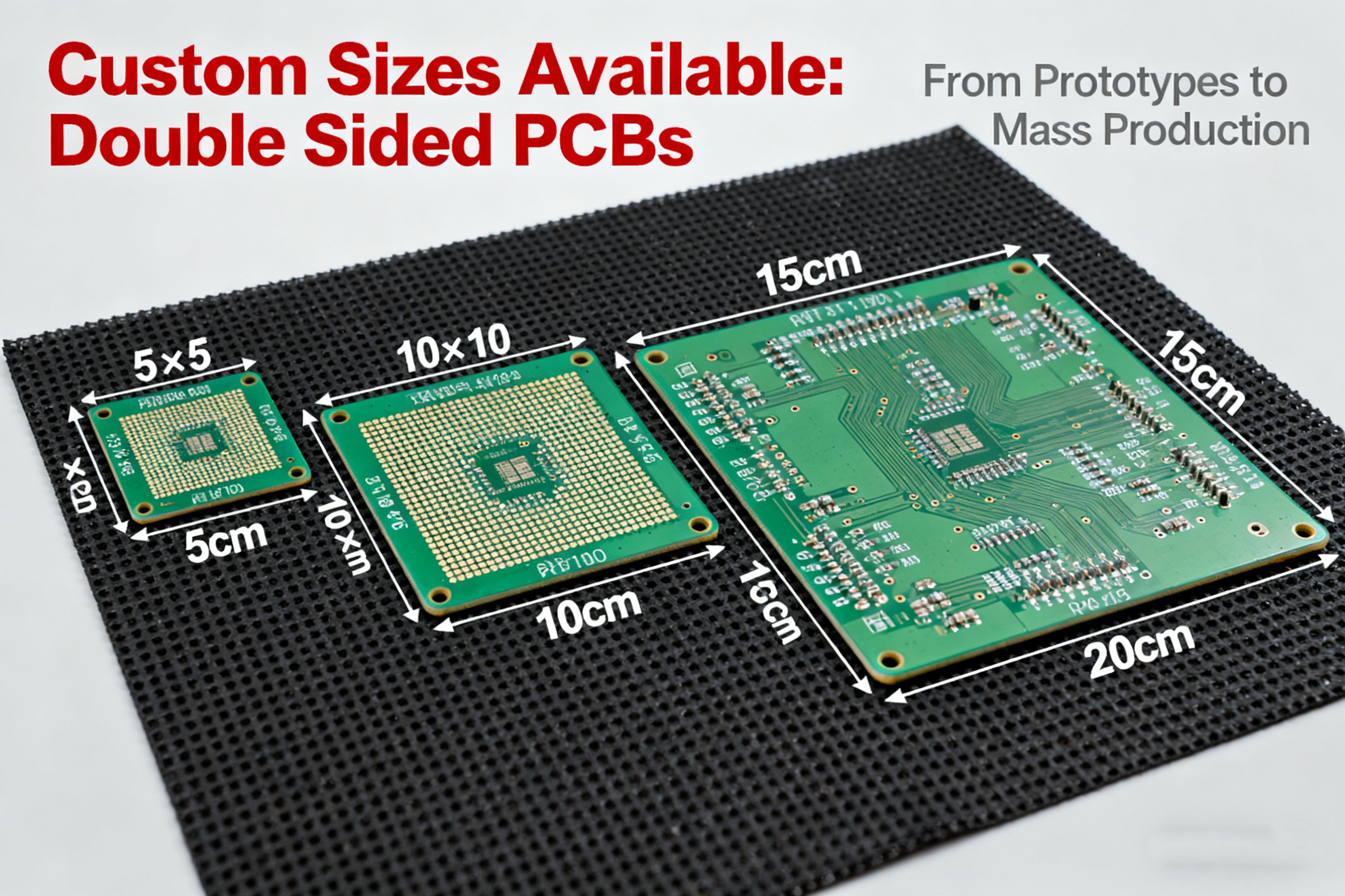
Ready to Start Your Double Sided PCB Project?
Submit Your Design File for a Free Quote & DFM Analysis in 24 Hours!