1. What is a multilayer PCB stackup?
Typically, when designing standard single- or double-sided boards, PCB stackup considerations are unnecessary. One usually selects laminates with copper thickness and board thickness meeting design requirements for direct processing. However, when designing PCBs with four or more layers, stackup design directly impacts both performance and cost.
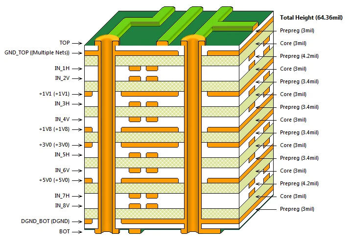
Multilayer PCBs are manufactured by laminating copper-clad core boards, prepreg (PP), and copper foil according to the stackup design through a compression process.
Before PCB design commences, layout engineers determine the number of layers based on board dimensions, circuit scale, and EMC requirements. They then establish component placement and finalize the division of signal layers, power planes, and ground planes.
2. PCB Laminate Design Principles
PCB laminate design requires consideration of multiple factors, including layer count, signal type, board thickness, material selection, copper thickness, impedance control, EMI/EMC shielding, thermal management, cost, and testability.
Meeting Signal Integrity Requirements for High-Speed Signal Routing
For critical signal traces, a GND/Signal/GND stackup configuration must be implemented. Adjacent signal layers should utilize striplines with perpendicular routing to minimize crosstalk coupling. From a signal integrity perspective, critical high-speed signals should employ stripline routing, while non-critical high-speed signals may opt for microstrip routing.
Broadside-coupled striplines are not recommended unless absolutely necessary. Offsets during PCB exposure and etching processes can cause misalignment, making fabrication difficult and compromising impedance consistency.
Selection of PCB Substrates, Polypropylene, and Copper Foil
FR-4 meets most PCB requirements with its low cost and good electrical performance. High-speed PCBs typically use high-speed materials like Panasonic's Megtron 4/6. RF PCBs employ carbon-hydrogen, Teflon, or ceramic substrates. Designs with high thermal dissipation demands, such as automotive light boards, utilize aluminum or copper substrates. Glass substrates are common in display applications like Mini LED.
| PCB Board Specifications | |
| Electrical Properties | Dielectric loss factor (df) |
| Dielectric constant (dk) | |
| Withstand voltage | |
| Physical properties | Glass Transition Temperature (Tg) |
| Thermal Decomposition Temperature (Td) | |
| Relative Creepage and Tracking Index (CTI) | |
| CAF Resistance | |
| Water Absorption | |
| Flammability | |
| Thermal Conductivity | |
| Mechanical Properties | Copper Foil Peel Strength |
| Flexural Strength | |
| Thermal Stress | |
High-Speed PCB Material Selection
High-speed PCBs require dielectric materials with the lowest loss tangent and minimal dielectric constant. Designing high-speed PCBs demands particular attention to material specifications, including fiberglass, dielectric matrix, and copper. Signals at higher data rates exhibit higher frequency components and shorter wavelengths, where impedance discontinuities generate increased reflections. Considerations include the effects of the glass weave pattern and copper foil surface roughness.
Glass Fiber Effect Introduced by Glass Fiber Cloth
Different glass fibers exhibit varying weave densities, window thicknesses, and interweaving thicknesses. When signals are routed over windows versus glass fibers, their characteristics (impedance, delay, loss) differ (due to distinct Dk/Df properties between windows and glass fibers). This phenomenon is known as the glass fiber effect.
Methods to mitigate the glass fiber effect:
Select glass fiber materials with minimized resin windows.
Employ routing techniques like Zig-Zag at 10° angles.
Request the PCB manufacturer to rotate the board by a specific angle during fabrication.
Use flat-weave or plain-weave glass cloth.
Copper Roughness
Copper roughness (copper pits) causes uneven trace width and spacing, leading to uncontrollable impedance. Additionally, due to the skin effect, current concentrates near the conductor surface. Copper surface roughness affects signal propagation length.
3. Copper Thickness per PCB Layer
PCB copper foil thickness is measured in ounces (oz). Common thicknesses include 0.5 oz (inner layers), 1 oz (outer layers), and 2 oz, primarily used in consumer and communication products. Thick copper exceeding 3 oz is typically employed in high-voltage, high-current power electronics.
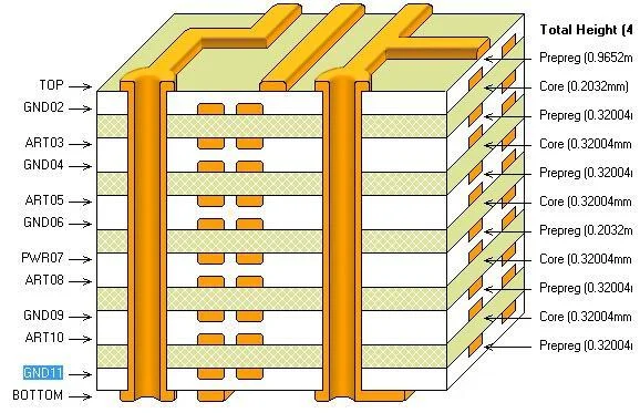
Layer stackup design must balance copper thickness to ensure power/ground plane layers meet current-carrying requirements. For signal layer copper thickness, smaller line widths/spacing necessitate thinner copper to meet precise etching requirements. High-speed signal traces experience skin effect, where current flows primarily near the copper foil surface. Thicker copper does not improve performance. Thus, the inner layer signal copper is typically 0.5 oz.
Layer Impedance Control
Many interface signal traces on PCBs have impedance requirements, such as common single-ended 50Ω or differential 100Ω. Impedance control necessitates a reference plane, typically requiring four or more layers.
Impedance mismatch causes signal distortion, reflections, and radiation—signal integrity issues that degrade PCB performance. Trace parameters like copper thickness, dielectric constant, width, and spacing all affect impedance. We can calculate impedance using EDA tools and adjust trace parameters based on the designed layer stackup. Most standard PCB manufacturers can achieve impedance control within 10%.
4. Layer Stackup Via Structure
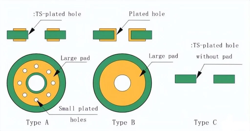
Through-Holes (PTH) penetrate the entire PCB, connecting all layers. Blind Vias connect outer layers to one or more inner layers without traversing the PCB. Buried Vias connect only inner layers.
High-density interconnect (HDI) PCBs frequently employ blind and buried vias to optimize routing space. However, these vias necessitate multiple lamination steps, increasing manufacturing complexity and cost.
During laminate design, the overall via structure should be planned according to design requirements. Where feasible, simplify via configurations while maintaining design integrity.
5. EMC Design for PCB Laminates
PCB stackup EMC design follows these principles:
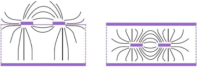
Power planes and ground planes should be positioned as close as possible to each other within the board, typically with the ground plane above the power plane. This design effectively utilizes interlayer capacitance as smoothing capacitance for the power supply while shielding the radiated currents distributed from the power plane.
Power and ground planes should be allocated to inner layers. The ground plane can function as a shielding layer, effectively suppressing inherent common-mode RF interference on the board and reducing the distributed impedance of high-frequency power sources.
Routing layers should be positioned adjacent to power or ground planes whenever possible to generate flux cancellation effects.
6. Thermal Design of PCB Laminates
PCB stackup design must incorporate thermal management to ensure efficient heat dissipation from components, preventing thermal damage and enhancing circuit reliability. During the design process, thermal simulation is first conducted based on component power dissipation. Based on simulation results, the component layout is optimized, and corresponding heat dissipation solutions are designed.
During the stackup design phase, targeted thermal design measures can also be implemented:
Prioritize substrates with high thermal conductivity; select metal core boards as needed;
Design heat sinks beneath high-power components and utilize heat dissipation holes;
Embed copper blocks and pillars to enhance thermal conduction efficiency;
Increase ground planes and fill unused areas with ground planes to expand the heat dissipation surface area.
Board Thickness Control
Standard PCB thicknesses include 0.5mm, 0.8mm, 1.0mm, 1.2mm, 1.6mm, 2.0mm, 3.2mm, 6.4mm, etc. Smaller boards typically use thinner materials, while larger boards subjected to frequent insertion/removal or high mounting stress require thicker materials for structural reliability.
7. PCB Laminate Design Steps
PCB laminate design generally follows these steps:
1. Determine the total stackup thickness (board thickness);
2. Define the number of PCB layers and allocate signal layers, ground planes, and power planes;
3. Specify copper thickness for inner and outer layers;
4. Determine impedance trace distribution;
5. Determine the via structure;
6. Determine the copper fill rate for each layer, preferably symmetrical;
7. Select substrate, PP, and copper foil materials that meet design requirements.
Benchuang Electronics offers high-quality Multilayer PCB services. Contact us and send your specifications.

