With the massive increase in system design complexity and integration, electronic system designers are now working on circuits operating above 100MHz. Bus operating frequencies have reached or exceeded 50MHz, with some even surpassing 100MHz. Currently, approximately 50% of designs feature clock frequencies exceeding 50MHz, and nearly 20% have main frequencies exceeding 120MHz.
When systems operate at 50 MHz, transmission line effects and signal integrity issues arise. At 120 MHz clock speeds, PCBs designed using traditional methods will fail unless high-speed circuit design expertise is applied.

Consequently, high-speed circuit design techniques have become essential tools for electronic system designers. Only through the application of high-speed design methodologies can the design process be effectively controlled.
What is a high-speed PCB circuit?
It is generally accepted that digital logic circuits operating at frequencies of 45 MHz to 50 MHz or higher, where circuits functioning at these frequencies constitute a significant portion (e.g., one-third) of the entire electronic system, are classified as high-speed circuits.
In reality, the harmonic frequencies of signal edges exceed the signal's fundamental frequency. Rapid transitions during signal rise and fall edges (or signal transitions) trigger unintended consequences in signal propagation. Therefore, it is generally agreed that if the line propagation delay exceeds half the rise time of the digital signal's driving edge, such signals are considered high-speed and exhibit transmission line effects.
Signal transmission occurs instantaneously during state transitions, such as rise or fall times. Signals travel from the driver to the receiver over a fixed duration. If the propagation time is less than half the rise or fall time, the reflected signal from the receiver will arrive at the driver before the signal state changes. Conversely, the reflected signal will arrive after the state change. If the reflected signal is sufficiently strong, the superimposed waveform may alter the logic state.

Determining High-Speed Signals
Above, we defined the prerequisites for transmission line effects. But how do we determine if the line delay exceeds half the signal rise time at the driver end? Typically, the rise time is specified in device manuals, while the propagation delay in PCB design depends on the actual routing length. The figure below shows the relationship between signal rise time and permissible routing length (delay).

The delay per inch on a PCB is 0.167 ns. However, delays increase with numerous vias, device pins, and net constraints. High-speed logic devices typically have a signal rise time of approximately 0.2 ns. If the board contains GaAs chips, the maximum routing length is 7.62 mm.
Let Tr denote the signal rise time and Tpd denote the propagation delay of the signal line. If Tr ≥ 4Tpd, the signal falls within the safe region. If 2Tpd ≥ Tr ≥ 4Tpd, the signal falls within the uncertain region. If Tr ≤ 2Tpd, the signal falls within the problematic region. For signals falling within the uncertain or problematic regions, high-speed routing techniques should be employed.
What is a Transmission Line
The traces on a PCB board can be equivalently modeled as the series and parallel capacitance, resistance, and inductance structures shown in the diagram below. The typical value for series resistance is 0.25-0.55 ohms/foot.
Due to the insulating layer, the parallel resistance value is usually very high. After adding parasitic resistance, capacitance, and inductance to the actual PCB trace, the resulting impedance along the trace is called the characteristic impedance Zo. Zo decreases as the trace width increases, the trace approaches the power/ground plane, or the dielectric constant of the isolation layer rises.
If the transmission line and receiving end have mismatched impedances, the output current signal and the signal's final steady state will differ. This causes reflections at the receiving end, where the reflected signal travels back to the signal source and reflects again. As energy diminishes, the reflected signal's amplitude decreases until the signal's voltage and current stabilize. This effect is called oscillation, and signal oscillations are often visible on both the rising and falling edges of the signal.
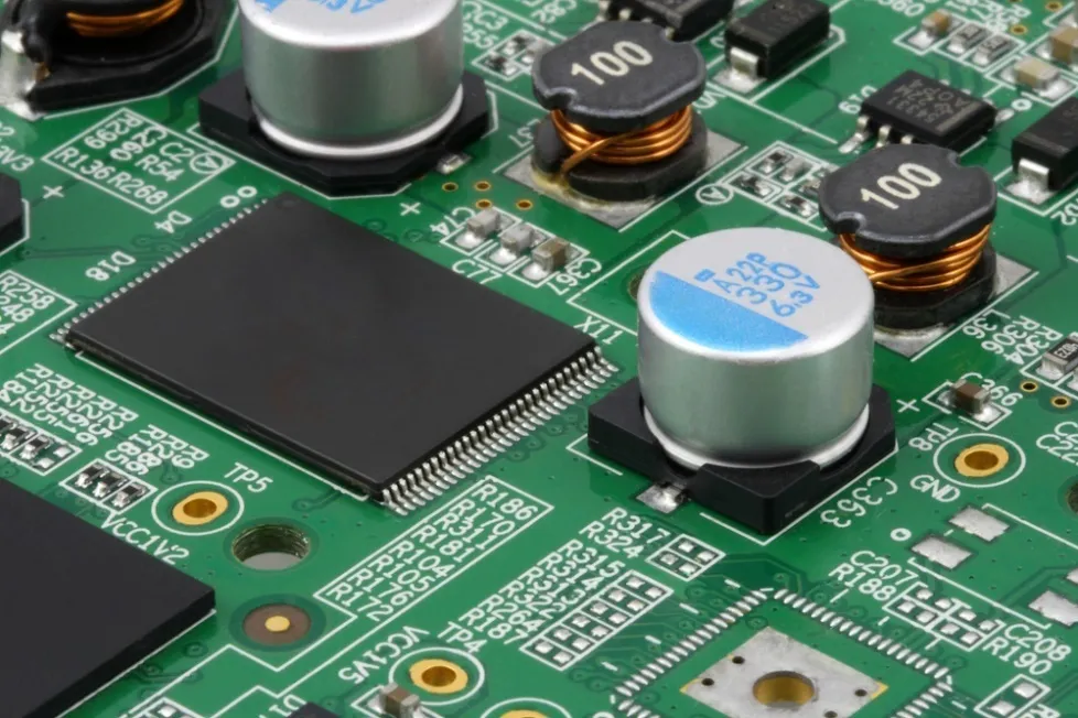
Benchuang Electronics offers high-quality PCB design and layout services. Contact us and send your specifications.

