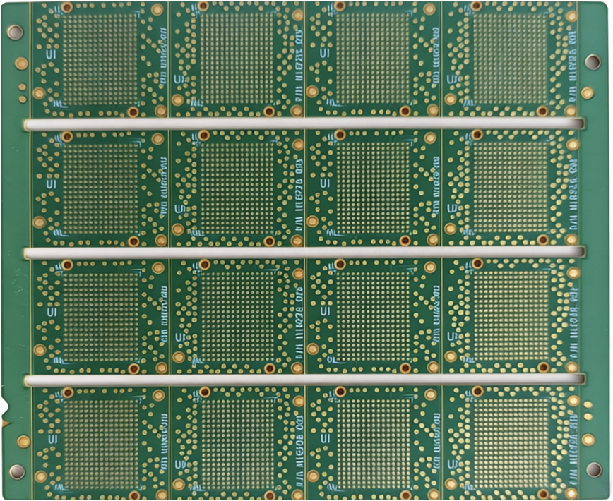
Engineered for direct IC chip mounting and high-speed signal interconnection. Supporting 1-20 layers with microvias and fine trace/space down to 0.05mm, ultra-thin profiles, and exceptional heat dissipation. From prototype to mass production in just 7-15 days
Core Advantages
Ultra-High Density & Fine Pitch
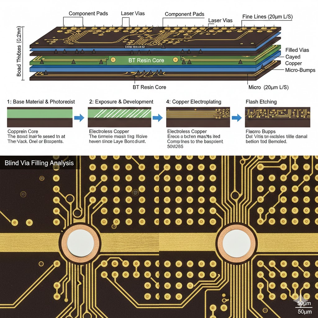
Microvias and trace/space as fine as 0.05mm enable complex routing for advanced IC packaging. Perfect bridge between chip and main PCB for maximum integration.
Superior Signal Integrity & High-Speed Performance
Optimized for RF and high-frequency applications with low-loss materials — ideal for 5G modules, AI processors, and high-performance computing.
Excellent Thermal Management
Advanced materials and designs dissipate heat efficiently from power-hungry chips, ensuring reliability in automotive ADAS, EV battery systems, and industrial equipment.
Miniaturization & Reliability
Ultra-thin, lightweight substrates with 19 years of proven high-reliability fabrication. Withstands extreme environments for aerospace, medical implants, and semiconductor devices.
Trending Applications
Our Precision Substrate Solutions Serving global clients in semiconductor and electronics since 2007 with custom IC substrates and full turnkey PCBA.
Semiconductor & AI Hardware : CPU/GPU packaging, AI accelerators, high-compute modules
5G & Communications : Base station chips, RF modules, high-frequency interconnects
Automotive & New Energy Vehicles : ADAS sensors, EV power management ICs, battery controllers
Medical Electronics : Implantable devices, diagnostic imaging chips, patient monitoring
Aerospace & Industrial Control : Avionics, satellite modules, robot controllers, energy systems
Consumer Electronics : Smartphones, wearables, drones with advanced chip packaging
Our Factory's Manufacturing Capabilities
Shenzhen Benchuang Precision Electronics Co., Ltd. — 19 years dedicated to high-density PCB & IC substrate manufacturing since 2007. Imported equipment, full in-house engineering, and one-stop PCBA services.
1-20 Layer Range
0.05mm Min Trace/Space
Ultra-Thin Profiles
Microvia & HDI Support
Materials & Processes
• High-Tg FR-4 / Low-Loss / Ceramic-Filled Substrates
• Rolled Annealed Copper Foils
• HDI / RF / Rigid-Flex Compatible Designs
• ENIG / OSP / Immersion Gold / Advanced Surface Finishes
Dimensions & Tolerances
• Max Panel Size Supporting Complex IC Packages
• Thickness Tolerance ±0.03mm
• Precise Solder Mask & Alignment for Fine-Pitch ICs
• Stiffener & Thermal Via Options
Service Capabilities
• 24-Hour Rapid Prototyping for IC Substrates
• Small Batch to Million-Level Production
• One-Stop Turnkey PCBA: SMT + THT, BGA/QFN, AOI/ICT/Functional Testing
• Full DFM Review, Layout Support, and Global Logistics
Production Process - From Design to Delivery in Just 7-15 Days
01 Requirements Discussion - GERBER / IC Spec Confirmation
02 Engineering Prototyping - 48 Hours First Substrate
03 Sample Validation - Signal / Thermal / Reliability Testing
04 Mass Production Optimization - Free DFM Report
05 On-Time Delivery - Global Logistics Tracking
Ready to Launch Your IC Substrate Project?
Contact Us Email: william@bcpcbsz.com. Our engineers will reply with a quote within 2 hours (weekdays).