China Multilayer High Frequency PCB : Micro Server PCB
As processing power hits new heights, the Micro Server PCB has become the defining factor in hardware reliability. Standard boards often fail under the extreme thermal and signal demands of modern Edge AI. We provide high-tier HDI and Copper Inlay solutions designed to eliminate downtime and bridge the gap between complex prototypes and stable, high-yield mass production.
In the world of high-performance computing, shrinking massive throughput into a palm-sized Micro Server PCB is more than a packaging feat—it is a significant engineering bottleneck. While many R&D teams find success with bench-top prototypes, they often encounter system throttling, data packet loss, or hardware failure once the units are deployed under full-load conditions.
Industry data suggests that nearly 80% of micro server projects fail to reach successful mass production due to two critical oversights: Thermal Management and Signal Integrity (SI).
1. The Critical Pain Points: Why Standard PCBs Fail
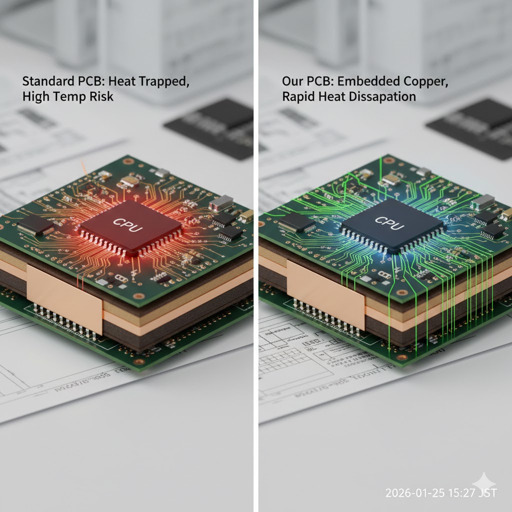
The Thermal Trap: Localized Hotspots
Micro servers operate in high-density environments with minimal airflow. When the SoC or FPGA hits peak load, heat must be evacuated through the PCB substrate. Inadequate thermal paths in a Micro Server PCB lead to "hotspots," triggering thermal throttling (CPU downclocking) or even delamination of the board layers due to thermal stress.
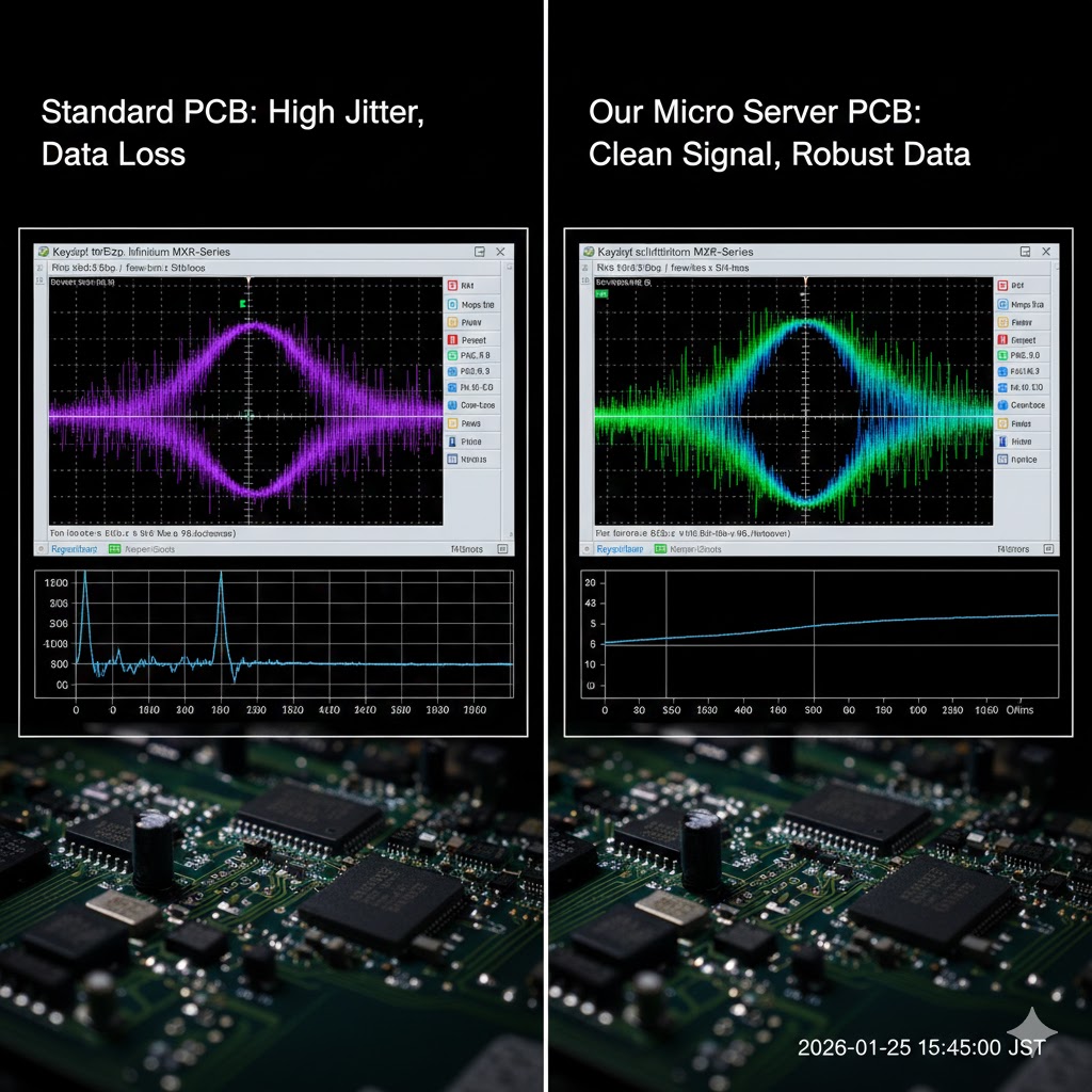
The SI Gap: Crosstalk in HDI Layers
Packing PCIe 5.0 lanes and DDR5 buses into tight stackups creates massive Electromagnetic Interference (EMI) risks. Without rigorous impedance control and advanced layer transitions, the result is persistent Bit Error Rates (BER) and unpredictable system instability.
2. Our Micro Server PCB Solutions: Engineering-First Fabrication
We provide a validated ecosystem designed to mitigate these risks before you hit the production line. Our process focuses on three core pillars:
Advanced Thermal Management (Copper Inlay): We embed solid copper blocks directly beneath high-wattage components. This achieves thermal conductivity 400% higher than standard thermal vias, keeping your silicon in the optimal temperature zone.
Precision Impedance Control (±5%): We maintain tolerances at ±5%—twice as strict as the industry standard (±10%). This ensures that high-speed differential pairs maintain absolute consistency across every production lot.
High-Tier HDI & Back-Drilling: We support Any-Layer HDI and automated back-drilling to eliminate via stubs. This ensures clean "eye diagrams" and maximum signal clarity at 32Gbps+ speeds.
3. Technical Specifications
Feature
Professional Micro Server PCB
Layer Count
2 - 32 Layers (HDI Any-Layer)
Base Materials
Megtron 6/7, Isola I-Speed, Rogers
Impedance Tolerance
±5%
Min. Trace/Space
2.5 mil (0.0635 mm)
Advanced Process
Copper Inlay, Back-drilling, Stacked Vias
4. Case Study: Slashing Core Temperatures by 18°C
The Challenge: A European edge-computing client faced persistent system crashes in outdoor deployments due to heat accumulation.
The Intervention: We re-engineered the 8-layer stackup using Isola Low-Loss laminates and integrated a strategic copper-inlay distribution.
The Result: Core operating temperatures dropped by 18°C. System reliability (MTBF) tripled, and the project successfully transitioned to a 10,000-unit mass production run.
5. Accelerate Your Time-to-Market (TTM)
Don't let a layout oversight be the reason your project stays in the lab. Partner with an engineering team that understands the rigors of high-density computing and Micro Server PCB fabrication.
We offer a comprehensive Design for Manufacturing (DFM) Review to catch potential SI and Thermal issues before you pull the trigger on production.