Thermal Integrity Without Compromise: Eliminate Field Failures in High-Power Modules
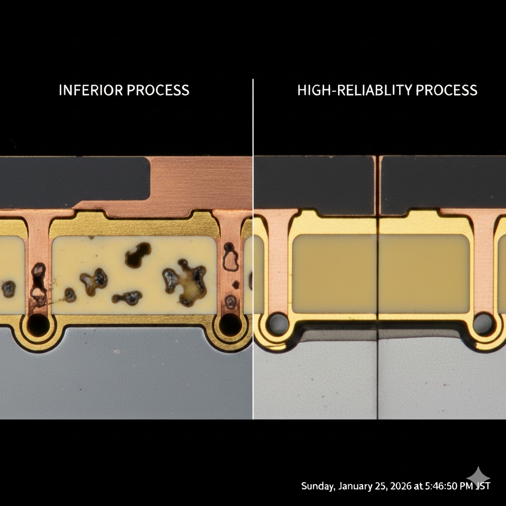
Thermal reliability shouldn't be a guessing game. At Benchuang, we engineer high-conductivity PCBs that bridge the gap between your FEA simulations and real-world durability. We don't just manufacture boards; we eliminate the thermal bottlenecks that cause field failures, ensuring your power modules run cooler, longer, and safer.
1. The Real Cost of Thermal Mismanagement
In high-performance power electronics, cooling isn't just a requirement—it’s the cornerstone of your brand’s reliability. Whether you are engineering 800V EV Inverters, 5G Small Cells, or Industrial Power Blocks, even a $5^{\circ}\text{C}$ deviation from your thermal model can trigger catastrophic field recalls.
At Benchuang, we don't just "make boards." We bridge the gap between your FEA simulations and real-world durability. We solve the thermal bottlenecks that standard shops ignore, ensuring your product hits the market with zero reliability debt.
2. Engineering Out the Failure Points
A. Solving CTE Mismatch and Solder Fatigue
Rigid aluminum substrates expand at a different rate than ceramic components, leading to micro-cracks in solder joints over time.
The Solution: We utilize Low-CTE Dielectrics and "Stress-Buffer" bond-ply materials that synchronize thermal expansion across the stack-up.
The ROI: Extended component lifespan ($100,000+$ hours) and superior performance under extreme thermal cycling ($-40^{\circ}\text{C}$ to $+125^{\circ}\text{C}$).
B. Vacuum-Lamination: Zero Air Voids, Zero Hotspots
Micro-voids trapped in the dielectric layer act as thermal insulators, causing localized heat spikes that lead to dielectric burn-through.
The Solution: Our High-Pressure Vacuum Lamination process achieves $99.9\%$ surface wetting, eliminating air pockets entirely.
The ROI: A seamless thermal path that maintains dielectric integrity under high voltage and high heat, preventing "silent" field failures.
C. 6kV+ Isolation: Safety That’s Audit-Ready
For power grids and automotive systems, isolation failure is not an option.
The Solution: We provide 100% Hi-Pot verification at the panel level, ensuring your high-voltage creepage and clearance distances are strictly maintained.
The ROI: Guaranteed compliance with UL, TUV, and CE standards on the first pass. No redesigns. No liability risks.
3. Case Study: SiC Inverter Performance Recovery
The Challenge: A manufacturer of ultra-fast EV chargers saw MOSFET temperatures spiking beyond safe limits, forcing the system to throttle power by 30%.
The Intervention: We re-engineered their stack-up using a Copper-Base MCPCB with an ultra-thin $4.0\text{ W/m·K}$ dielectric and optimized resin-filled thermal vias.
The Result: Junction temperatures dropped by $18^{\circ}\text{C}$, allowing the client to maintain $100\%$ power throughput and secure a tier-1 automotive contract.
4. Technical Capabilities at a Glance
Engineering Challenge
Benchuang Solution
Why It Matters
High Current Density
Up to 12oz Heavy Copper
Minimizes $I^2R$ losses and prevents trace overheating.
Logic/Power Integration
Multilayer MCPCB (up to 4L)
Reduces footprint while maximizing thermal paths.
Dielectric Strength
$3\text{kV}$ – $10\text{kV}$ AC/DC
Absolute safety for high-voltage EV/Industrial apps.
Mechanical Stress
Flexible Thermal Bond-Ply
Dampens vibration and absorbs CTE-related stress.
5. Why Leading R&D Teams Partner with Us
Material Integrity: We source exclusively from industry-standard laminates (Bergquist, Ventec, Laird). No generic substitutes that degrade over time.
Design-for-Manufacturing (DFM): We don't just take orders. We review your stack-up for thermal efficiency and provide optimization feedback within 12 hours.
Rapid Deployment: High-reliability thermal prototypes delivered in 5–7 business days.
6. Get Your Design Peer-Reviewed
Don't let a $0.05\text{mm}$ air void sink your project. Send us your Gerber files and thermal requirements for a complimentary Thermal Stack-up Review.