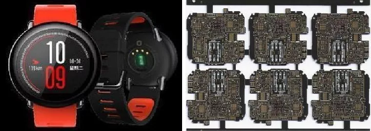
As 5G commercialization accelerates globally, the demand for wireless communication infrastructure—especially base stations—has surged dramatically. Behind this boom lies a critical component: Printed Circuit Boards (PCBs). 5G networks rely on high-performance PCBs for core communication equipment such as switches, routers, and optical transport systems. Unlike 4G, 5G imposes unprecedented demands on PCBs: ultra-high reliability, superior electrical and thermal performance, strict product quality control, and a lifespan of over a decade. For PCB manufacturers, mastering these advanced technologies is not just a challenge—it’s the key to unlocking the $100-billion-plus 5G PCB market.

The 5G-Driven PCB Technical Revolution: 4 Core Requirements
1. Via Technology: The Backbone of High-Density 5G PCBs
5G devices pack more functions into smaller spaces, pushing PCB density to new heights. This trend has made blind and buried vias (critical for HDI, High-Density Interconnect, designs) indispensable. While most manufacturers have mastered 1-3 level HDI, higher-level HDI with arbitrary interconnection sequences remains a gap—one that early adopters are rushing to fill.
Another pain point? Stub management. In 5G’s high-frequency environment, the “short-stub effect” degrades signal quality severely. This means back-drilling processes (to minimize stubs) are no longer optional—they’re a standard. Additionally, 5G’s high-frequency, high-power devices generate significant heat; embedding copper blocks within PCBs has become a go-to solution to enhance heat dissipation, ensuring long-term stability.
2. Circuit & Surface Technology: Precision for 56Gbps Signals
5G data transmission rates have jumped from 25Gbps to 56Gbps, placing brutal demands on impedance control and signal loss. For PCB manufacturers, this translates to:
- Tighter tolerances: Impedance tolerance has shrunk from ±10% to ±5%, and line width tolerance from ±20% to ±10%. Even minor deviations can disrupt signal integrity.
- Smoother surfaces: The “skin effect” (where high-frequency signals travel along conductor surfaces) makes copper foil roughness a critical factor. For inner layers, Ra (roughness average) must be <0.5μm to reduce signal loss.
- Uniform interlayers: Dielectric layer thickness uniformity (required to be ≤15%) directly impacts signal transmission. Key areas like large-copper-surface BGAs and impedance lines now require dedicated thickness control systems.
Every step—from board material selection to engineering design and manufacturing—must align to meet these precision standards.
3. Substrate Technology: Balancing Heat, Durability, and Compatibility
5G’s high-frequency operations push PCBs to their thermal limits. Here’s what manufacturers need to prioritize:
- Low dissipation factor (Df): As 5G frequencies rise, minimizing Df is non-negotiable to reduce signal attenuation.
- Superior heat resistance: Thin substrate materials, high thermal conductivity, and smooth copper foils are essential. PCB operating temperatures demand higher Relative Thermal Index (RTI)—a shift from 105°C to 150°C—and better Thermal Conductivity (Tc). Simulations prove: improving Tc is more effective than reducing Df at lowering temperature rise.
- Controlled expansion: For large PCBs (≥1100mm) and chips (≥100mm), compatibility with packaging materials requires PCB CTE (Coefficient of Thermal Expansion) in the X/Y axis to be ≤12PPM.
- High CTI: Power boards for 5G infrastructure need a high Comparative Tracking Index (CTI) to prevent electrical breakdown.
4. Auxiliary Materials: The “Hidden” Drivers of Signal Quality
Often overlooked, auxiliary materials can make or break 5G PCB performance:
- Solder mask ink: Conventional inks have become a bottleneck for outer high-speed circuits. Ultra-low-loss solder mask inks are urgently needed to preserve signal integrity—especially for black solder masks, which significantly impact high-frequency signals.
- Brown-coating solutions: High-frequency, high-speed signals are sensitive to copper foil roughness (due to the skin effect). Low-roughness brown-coating solutions are now widely adopted to minimize circuit loss in 5G PCBs.
Seize the 5G PCB Opportunity: 3 Actionable Strategies for Manufacturers
- Invest in HDI and Back-Drilling Capabilities: Partner with equipment suppliers to upgrade 4+ level HDI production lines and precision back-drilling machines—this will help you meet the high-density demands of 5G base stations and routers.
- Collaborate with Material Suppliers: Work closely with substrate and ink manufacturers to develop custom solutions (e.g., low-Df substrates, ultra-low-loss inks) tailored to 5G’s unique needs.
- Optimize Quality Control Systems: Implement real-time monitoring for impedance, dielectric thickness, and copper roughness. Certifications like IPC-6012 (for PCB quality) and ISO 9001 will build trust with 5G equipment OEMs.